CY22801 Ver la hoja de datos (PDF) - Cypress Semiconductor
Número de pieza
componentes Descripción
Fabricante
CY22801 Datasheet PDF : 7 Pages
| |||
CY22801
AC Electrical Characteristics[2]
Parameter
Name
Description
Min Typ Max Unit
fREFC
Reference Frequency -
crystal
8
–
30 MHz
fREFD
fOUT
Reference Frequency - driven
Output Frequency,
Commercial Grade
1
–
133 MHz
1
–
200 MHz
Output Frequency, Industrial
Grade
1
–
166.6 MHz
DC
Output Duty Cycle
Duty Cycle is defined in Figure 4, 50% of
45
50
55
%
VDD
t3
Output Rising Edge Slew 20% - 80% of VDD
Rate
0.8
1.4
–
V/ns
t4
Output Falling Edge Slew 80% - 20% of VDD
Rate
0.8
1.4
–
V/ns
t5[5]
Skew
Output-output skew between related
outputs
–
–
250
ps
t6[6]
Clock Jitter
t10
PLL Lock Time
Peak-to-peak period jitter
–
250
–
ps
–
–
3
ms
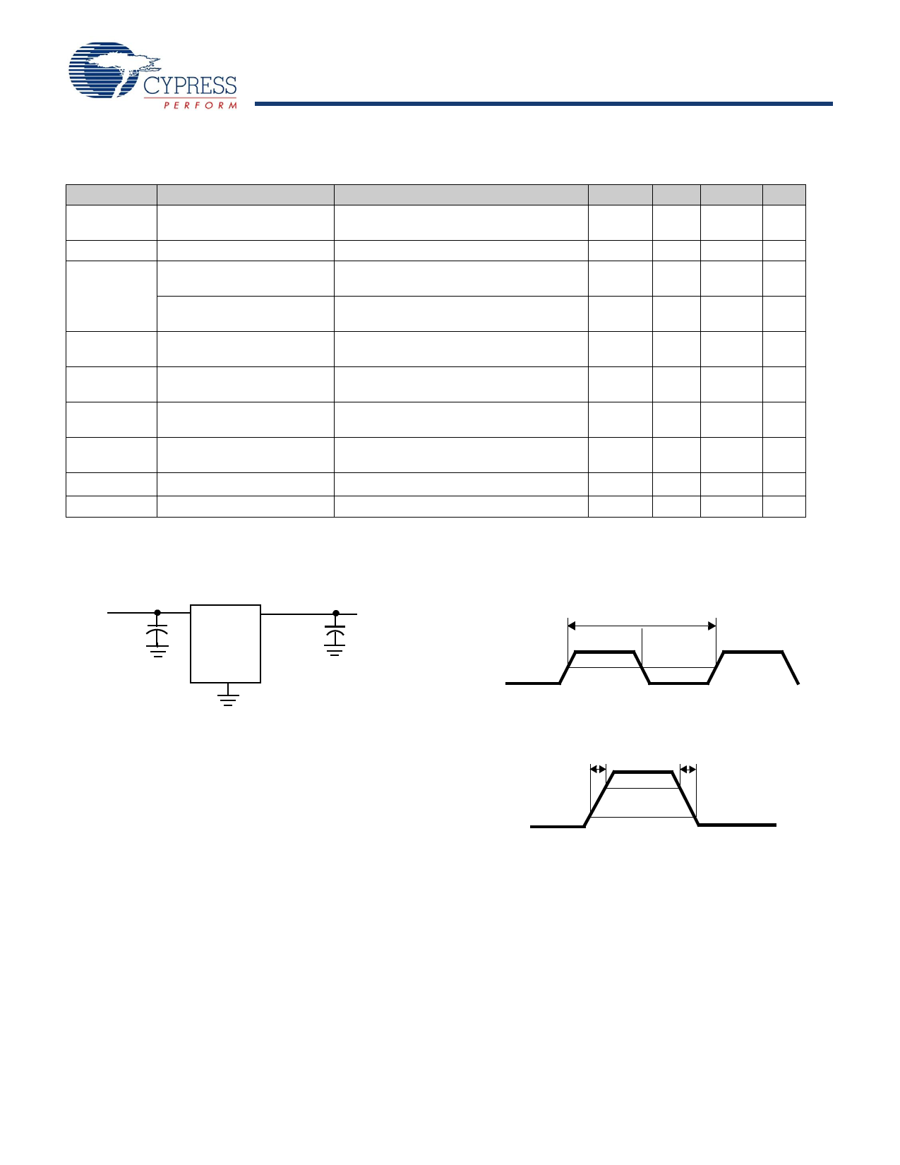
Test Circuit
Figure 3. Test Circuit Diagram
VDD
0.1 μF
OUTPUTS
CLKout
CLOAD
Timing Definitions
Figure 4. Duty Cycle Definition; DC = t2/t1
t1
t2
CLK
50%
50%
GND
Figure 5. Rise and Fall Time Definitions
t3
t4
80%
CLK
20%
Notes
5. Skew value guaranteed when outputs are generated from the same divider bank.
6. Jitter measurement may vary. Actual jitter is dependent on input jitter and edge rate, number of active outputs, input and output frequencies, supply voltage, temperature,
and output load. For more information, refer to the application note, Jitter in PLL-based Systems: Causes, Effects, and Solutions.
Document #: 001-15571 Rev. *B
Page 5 of 7
[+] Feedback
Share Link: 