CY14B104LA Ver la hoja de datos (PDF) - Cypress Semiconductor
Número de pieza
componentes Descripción
Fabricante
CY14B104LA Datasheet PDF : 23 Pages
| |||
CY14B104LA, CY14B104NA
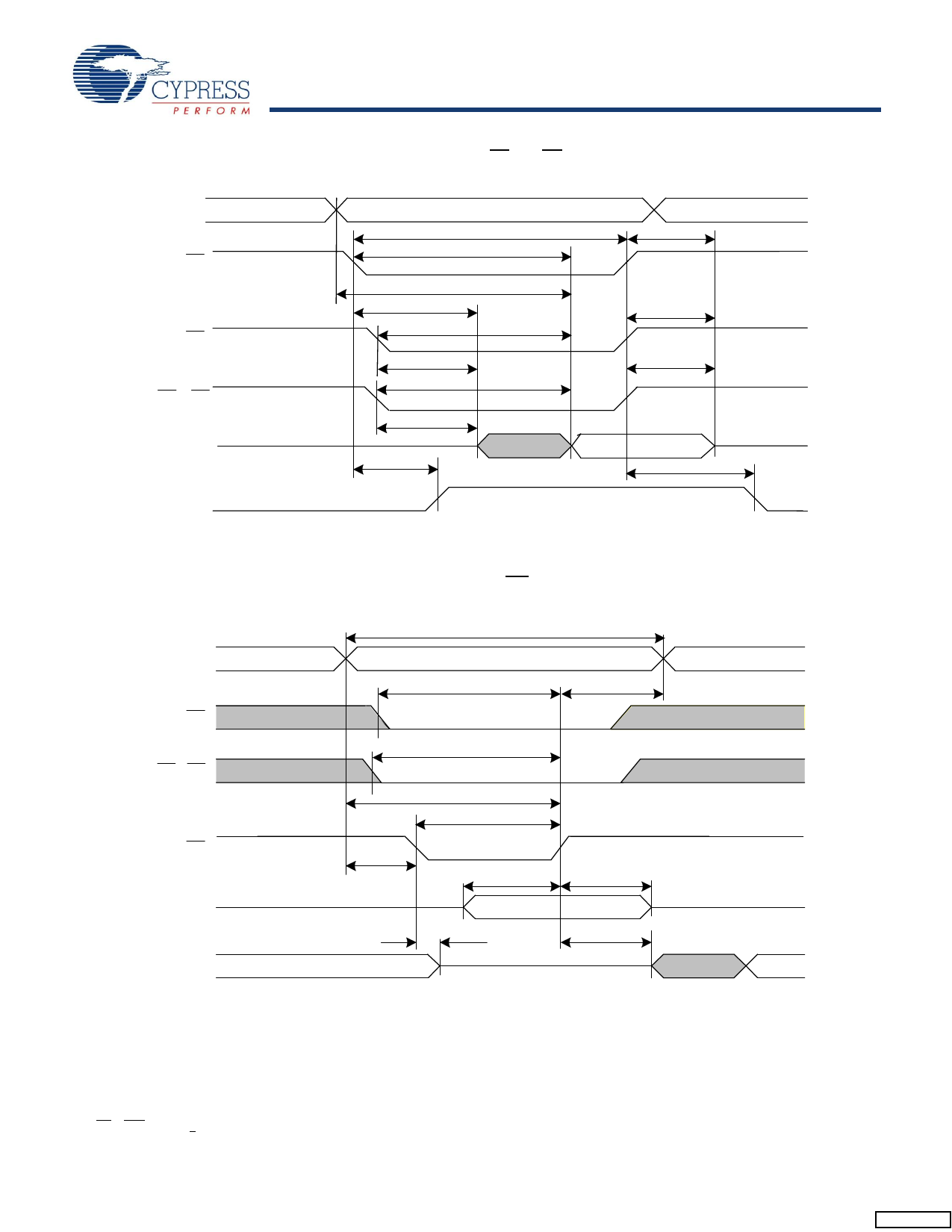
Figure 7. SRAM Read Cycle #2: CE and OE Controlled[3, 12, 16]
Address
CE
OE
BHE, BLE
Data Output
High Impedance
ICC
Standby
Address Valid
tRC
tACE
tAA
tLZCE
tLZOE
tDOE
tDBE
tLZBE
tPU
Active
tHZCE
tHZOE
tHZBE
Output Data Valid
tPD
Address
CE
BHE, BLE
WE
Data Input
Data Output
Figure 8. SRAM Write Cycle #1: WE Controlled[3, 15, 16, 17]
tWC
Address Valid
tSCE
tHA
tSA
Previous Data
tBW
tAW
tPWE
tHZWE
tSD
tHD
Input Data Valid
tLZWE
High Impedance
Note
17. CE or WE must be >VIH during address transitions.
Document #: 001-49918 Rev. *B
Page 11 of 23
[+] Feedback
Share Link: 