CY14B104LA-ZS45XI(2011) Ver la hoja de datos (PDF) - Cypress Semiconductor
NÚmero de pieza
componentes DescripciÃģn
Fabricante
CY14B104LA-ZS45XI Datasheet PDF : 24 Pages
| |||
CY14B104LA, CY14B104NA
Maximum Ratings
Exceeding maximum ratings may impair the useful life of the
device. These user guidelines are not tested.
Storage temperature ................................ â65 °C to +150 °C
Maximum accumulated storage time
At 150 °C ambient temperature..........................1000 h
At 85 °C ambient temperature.................... .. 20 Years
Ambient temperature with
power applied ........................................... â55 °C to +150 °C
Supply voltage on VCC relative to VSS............â0.5 V to 4.1 V
Voltage applied to outputs
in high-Z state...................................... â0.5 V to VCC + 0.5 V
Input voltage .........................................â0.5 V to Vcc + 0.5 V
Transient voltage (<20 ns) on
any pin to ground potential .................. â2.0 V to VCC + 2.0 V
Package power dissipation
capability (TA = 25 °C) ................................................. .1.0 W
Surface mount Pb soldering
temperature (3 Seconds).......................................... +260 °C
DC output current (1 output at a time, 1s duration) ..... 15 mA
Static discharge voltage.......................................... > 2001 V
(per MIL-STD-883, Method 3015)
Latch up current..................................................... > 200 mA
Operating Range
Range
Industrial
Ambient Temperature
â40 °C to +85 °C
VCC
2.7 V to 3.6 V
DC Electrical Characteristics
Over the Operating Range (VCC = 2.7 V to 3.6 V)
Parameter Description
Test Conditions
Min
VCC
Power supply
2.7
ICC1
Average VCC current tRC = 20 ns
â
tRC = 25 ns
tRC = 45 ns
Values obtained without output loads (IOUT = 0 mA)
ICC2
Average VCC current All inputs donât care, VCC = Max
â
during STORE
Average current for duration tSTORE
ICC3
Average VCC current All inputs cycling at CMOS levels.
â
at tRC= 200 ns,
Values obtained without output loads (IOUT = 0 mA).
VCC (Typ), 25 °C
ICC4
Average VCAP
All inputs donât care. Average current for duration tSTORE
â
current during
AutoStore cycle
ISB
IIX[13]
VCC standby current CE > (VCC â 0.2 V). VIN < 0.2 V or > (VCC â 0.2 V).
â
Standby current level after nonvolatile cycle is complete.
Inputs are static. f = 0 MHz.
Input leakage current VCC = Max, VSS < VIN < VCC
â1
(except HSB)
Input leakage current VCC = Max, VSS < VIN < VCC
(for HSB)
â100
IOZ
VIH
VIL
VOH
VOL
VCAP
Off-state output
leakage current
VCC = Max, VSS < VOUT < VCC, CE or OE > VIH or BHE/BLE â1
> VIH or WE < VIL
Input HIGH voltage
2.0
Input LOW voltage
Output HIGH voltage IOUT = â2 mA
Output LOW voltage IOUT = 4 mA
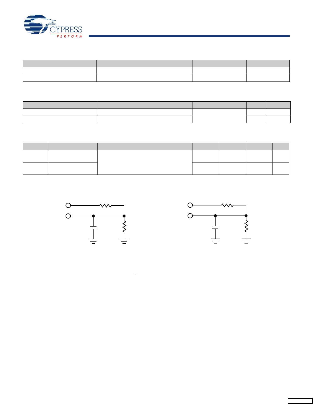
Storage capacitor Between VCAP pin and VSS, 5 V rated
Vss â 0.5
2.4
â
61
Typ[12]
3.0
â
â
35
â
â
â
â
â
â
â
â
â
68
Max Unit
3.6
V
70 mA
70 mA
52 mA
10 mA
â
mA
5
mA
5
mA
+1
ΞA
+1
ΞA
+1
ΞA
VCC + 0.5 V
0.8
V
â
V
0.4
V
180 ΞF
Notes
12. Typical values are at 25°C, VCC= VCC (Typ). Not 100% tested.
13. The HSB pin has IOUT = -2 uA for VOH of 2.4 V when both active HIGH and LOW drivers are disabled. When they are enabled standard VOH and VOL are valid. This
parameter is characterized but not tested.
Document #: 001-49918 Rev. *H
Page 9 of 24
[+] Feedback
Share Link: 