CY14B104LA-BA25XI(2011) Ver la hoja de datos (PDF) - Cypress Semiconductor
NГәmero de pieza
componentes DescripciГіn
Fabricante
CY14B104LA-BA25XI Datasheet PDF : 24 Pages
| |||
CY14B104LA, CY14B104NA
Pinouts (continued)
Figure 3. Pin Diagram - 54-Pin TSOP II (Г—16)
NC
[5]
1
NC 2
54 HSB
53 NC [4]
A0 3
52 A17
A1 4
51 A16
A2 5
A3 6
50 A15
49 OE
A4 7
48 BHE
CE 8
47 BLE
DQ0 9
46 DQ15
DQ1 10 54 - TSOP II 45
DQ2 11
(Г—16)
44
DQ3 12
43
VCC 13
Top View
42
VSS 14 (not to scale) 41
DQ4 15
40
DQ5 16
39
DQ14
DQ13
DQ12
VSS
VCC
DQ11
DQ10
DQ6 17
DQ7 18
WE 19
A5 20
A6 21
A7 22
A8 23
A9 24
NC 25
38 DQ9
37 DQ8
36
35
VCAP
A14
34 A13
33 A12
32 A11
31 A10
30 NC
NC 26
29 NC
NC 27
28 NC
Table 1. Pin Definitions
Pin Name I/O Type
Description
A0 вҖ“ A18
A0 вҖ“ A17
DQ0 вҖ“ DQ7
Input
Input/Output
Address inputs. Used to select one of the 524,288 bytes of the nvSRAM for x8 Configuration.
Address inputs. Used to Select one of the 262,144 words of the nvSRAM for x16 Configuration.
Bidirectional data I/O lines for Г—8 configuration. Used as input or output lines depending on
operation.
DQ0 вҖ“ DQ15
Bidirectional data I/O lines for Г—16 configuration. Used as input or output lines depending on
operation.
WE
Input
Write Enable input, Active LOW. When selected LOW, data on the I/O pins is written to the specific
address location.
CE
Input
Chip Enable input, Active LOW. When LOW, selects the chip. When HIGH, deselects the chip.
OE
Input
Output Enable, Active LOW. The active LOW OE input enables the data output buffers during read
cycles. I/O pins are tristated on deasserting OE HIGH.
BHE
BLE
VSS
VCC
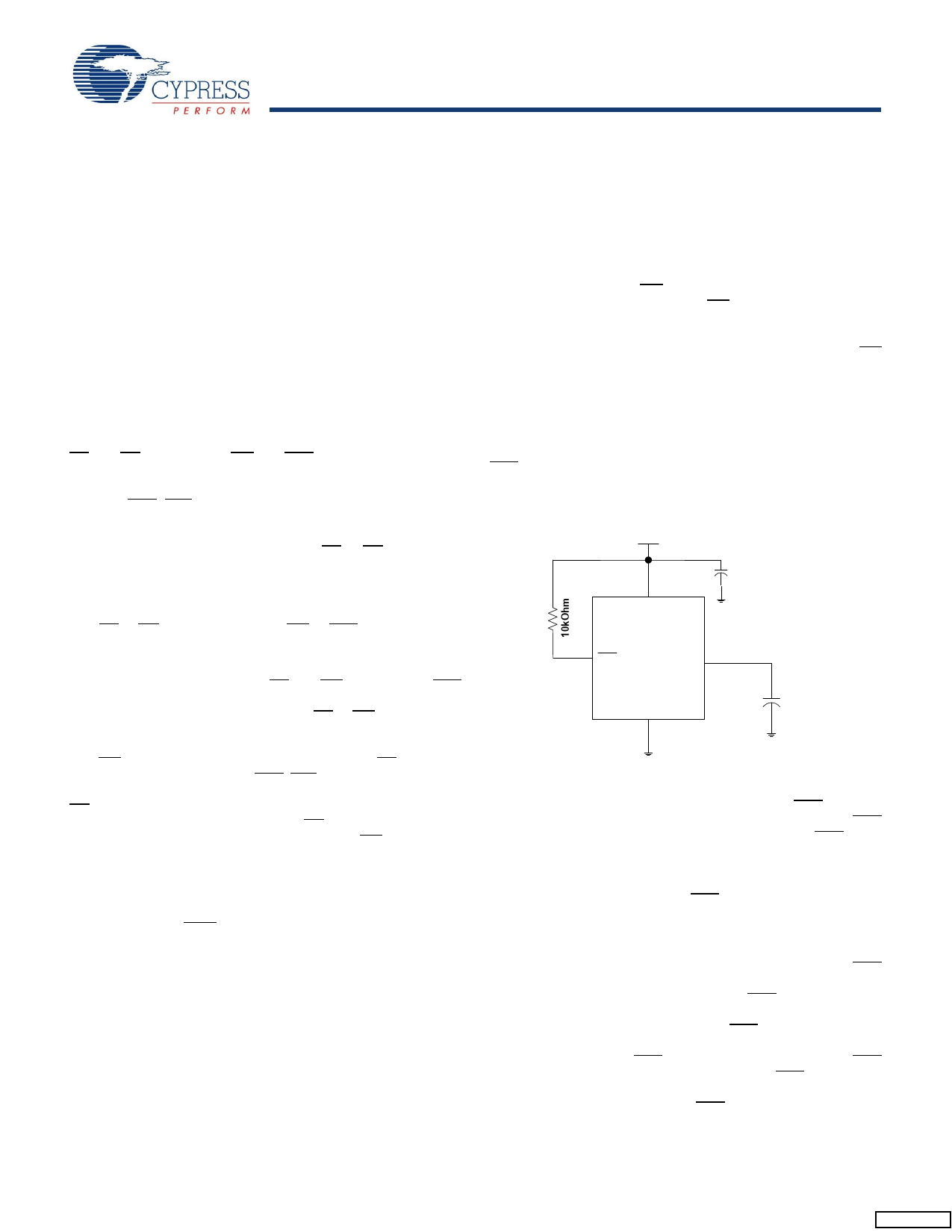
HSB[7]
Input
Input
Ground
Byte High Enable, Active LOW. Controls DQ15 - DQ8.
Byte Low Enable, Active LOW. Controls DQ7 - DQ0.
Ground for the device. Must be connected to the ground of the system.
Power supply Power supply inputs to the device.
Input/Output
Hardware STORE Busy (HSB). When LOW this output indicates that a Hardware STORE is in
progress. When pulled LOW external to the chip it initiates a nonvolatile STORE operation. After each
Hardware and Software STORE operation, HSB is driven HIGH for a short time (tHHHD) with standard
output high current, and then a weak internal pull-up resistor keeps this pin HIGH (external pull-up
resistor connection optional).
VCAP
Power supply AutoStore Capacitor. Supplies power to the nvSRAM during power loss to store data from SRAM to
nonvolatile elements.
NC
No connect No Connect. This pin is not connected to the die.
Note
7. HSB pin is not available in 44-TSOP II (Г—16) package.
Document #: 001-49918 Rev. *H
Page 4 of 24
[+] Feedback
Share Link: 