CY14B104K(2009) Ver la hoja de datos (PDF) - Cypress Semiconductor
Número de pieza
componentes Descripción
Fabricante
CY14B104K Datasheet PDF : 33 Pages
| |||
CY14B104K, CY14B104M
Pinouts
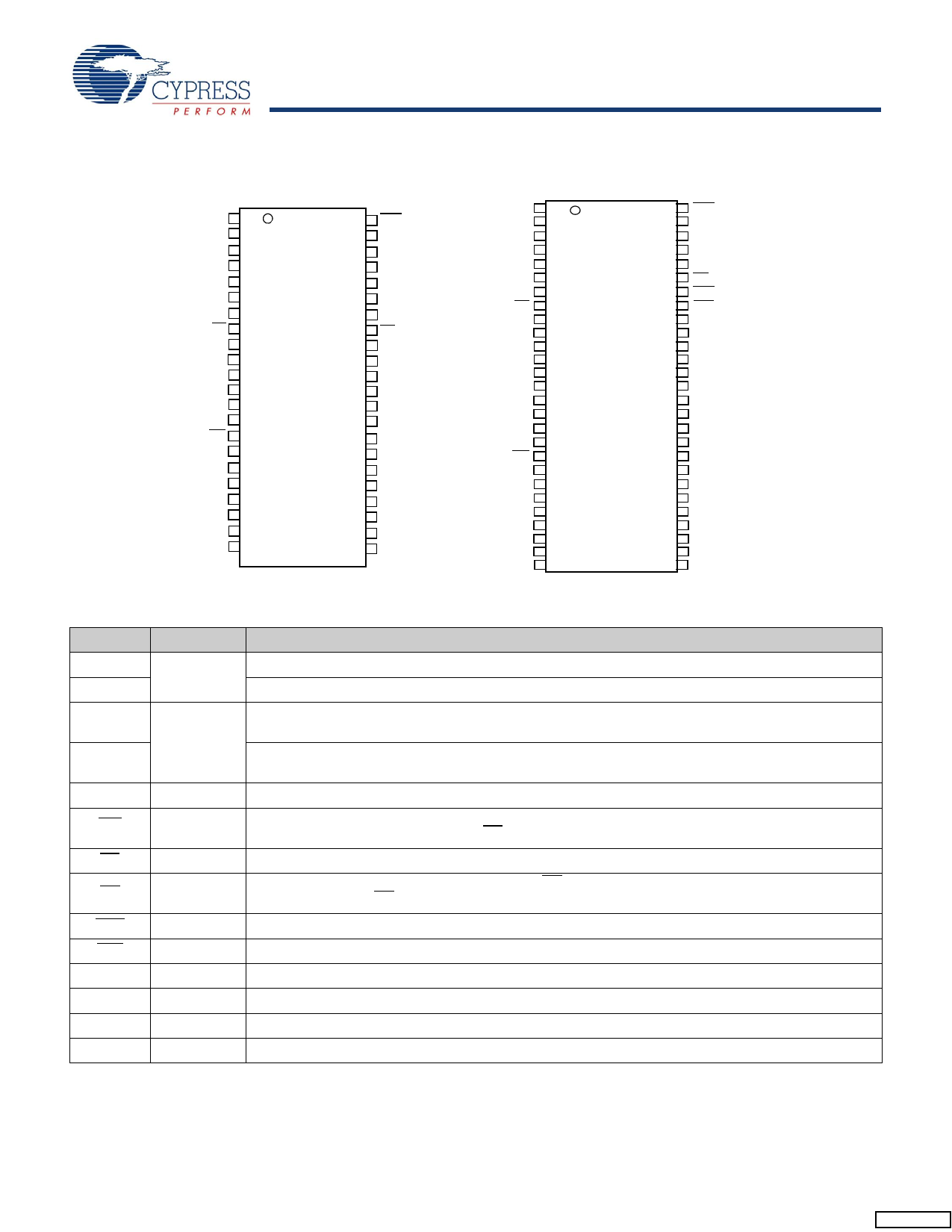
Figure 1. Pin Diagram - 44-PIn and 54-Pin TSOP II
INT 1
NC[5] 2
44
43
A0 3
42
A1 4
41
A2 5
40
A3 6
39
A4 7
38
CE 8
37
DQ0 9 44 - TSOP II 36
DQ1 10
(x8)
35
VCC 11
34
VSS
DQ2
12 Top View
13 (not to scale)
33
32
DQ3 14
31
WE 15
30
A5 16
29
A6 17
28
A7 18
27
A8 19
26
A9 20
25
Xout 21
24
Xin 22
23
HSB
NC[4]
NC
A18
A17
A16
A15
OE
DQ7
DQ6
VSS
VCC
DQ5
DQ4
VCAP
A14
A13
A12
A11
A10
VRTCcap
VRTCbat
IN[T5] 1
54
NC 2
53
A0 3
52
A1 4
51
A2 5
50
A3 6
49
A4 7
48
CE 8
47
DQ0 9
46
DQ1 10 54 - TSOP II 45
DQ2
DQ3
VCC
VSS
11
(x16)
44
12
43
13 Top View 42
14 (not to scale) 41
DQ4 15
40
DQ5 16
39
DQ6 17
38
DQ7 18
37
WE 19
36
A5 20
35
A6 21
34
A7 22
33
A8 23
32
A9 24
31
NC 25
30
Xout 26
29
Xin 27
28
HNSCB[4]
A17
A16
A15
OE
BHE
BLE
DQ15
DQ14
DQ13
DQ12
VSS
VCC
DQ11
DQ10
DQ9
DQ8
VCAP
A14
A13
A12
A11
A10
NC
VRTCcap
VRTCbat
Table 1. Pin Definitions
Pin Name I/O Type
Description
A0 – A18
A0 – A17
DQ0 – DQ7
Input
Input/Output
Address Inputs Used to Select One of the 524,288 bytes of the nvSRAM for x8 Configuration.
Address Inputs Used to Select One of the 262,144 words of the nvSRAM for x16 Configuration.
Bidirectional Data I/O Lines for x8 Configuration. Used as input or output lines depending on
operation.
DQ0 – DQ15
Bidirectional Data I/O Lines for x16 Configuration. Used as input or output lines depending on
operation.
NC
No Connect No Connects. This pin is not connected to the die.
WE
Input
Write Enable Input, Active LOW. When selected LOW, data on the I/O pins is written to the specific
address location.
CE
Input Chip Enable Input, Active LOW. When LOW, selects the chip. When HIGH, deselects the chip.
Input Output Enable, Active LOW. The active LOW OE input enables the data output buffers during read
OE
cycles. Deasserting OE HIGH causes the I/O pins to tristate.
BHE
BLE
Xout
Xin
VRTCcap
VRTCbat
Input
Input
Output
Byte High Enable, Active LOW. Controls DQ15 - DQ8.
Byte Low Enable, Active LOW. Controls DQ7 - DQ0.
Crystal Connection. Drives crystal on startup.
Input Crystal Connection. For 32.768 KHz crystal.
Power Supply Capacitor Supplied Backup RTC Supply Voltage. Left unconnected if VRTCbat is used.
Power Supply Battery Supplied Backup RTC Supply Voltage. Left unconnected if VRTCcap is used.
Notes
4. Address expansion for 8 Mbit. NC pin not connected to die.
5. Address expansion for 16 Mbit. NC pin not connected to die.
Document #: 001-07103 Rev. *M
Page 2 of 33
[+] Feedback
Share Link: 