CY14B101I(2012) Ver la hoja de datos (PDF) - Cypress Semiconductor
NГәmero de pieza
componentes DescripciГіn
Fabricante
CY14B101I
(Rev.:2012)
(Rev.:2012)
Cypress Semiconductor

CY14B101I Datasheet PDF : 41 Pages
| |||
PRELIMINARY
CY14C101I
CY14B101I
CY14E101I
Slave Device Address
Every slave device on an I2C bus has a device select address.
The first byte after START condition contains the slave device
address with which the master intends to communicate. The
seven MSBs are the device address and the LSB (R/W bit) is
used for indicating Read or Write operation. The CY14X101I
reserves three sets of upper 4 MSBs [7:4] in the slave device
address field for accessing the Memory, RTC Registers, and
Table 1. Slave Device Addressing
Control Registers. The accessing mechanism is described in the
following section.
The nvSRAM product provides three different functionalities:
Memory, RTC Registers and Control Registers functions (such
as serial number and product ID). The three functions of the
device are accessed through different slave device addresses.
The first four most significant bits [7:4] in the device address
register are used to select between the nvSRAM functions.
Bit 7 Bit 6 Bit 5 Bit 4 Bit 3
Bit 2
Bit 1
Bit 0
nvSRAM
Function Select
CY14X101I Slave Devices
1
0
1
0 Device select ID A16 R/W Selects Memory
Memory, 128 K Г— 8
1
1
0
1
Device select ID
X
R/W
Selects RTC
Registers
RTC Registers, 16 Г— 8
0
0
1
1
Device select ID
X
R/W
Selects Control
Registers
Control Registers
- Memory Control Register, 1 Г— 8
- Serial Number, 8 Г— 8
- Device ID, 4 Г— 8
- Command Register, 1 Г— 8
Memory Slave Device
The nvSRAM device is selected for read/write if the master
issues the slave address as 1010b followed by two bits of device
select. If the slave address sent by the master matches with the
Memory Slave device address then depending on the R/W bit of
the slave address, the data will be either read from (R/W = вҖҳ1вҖҷ) or
written to (R/W = вҖҳ0вҖҷ) the nvSRAM.
The address length for CY14X101I is 17 bits, and thus it requires
three address bytes to map the entire memory address location.
To save an extra byte for memory addressing, the 17th bit (A16)
is mapped to the slave address select bit (A0). The dedicated
two address bytes represent bit A0 to A15.
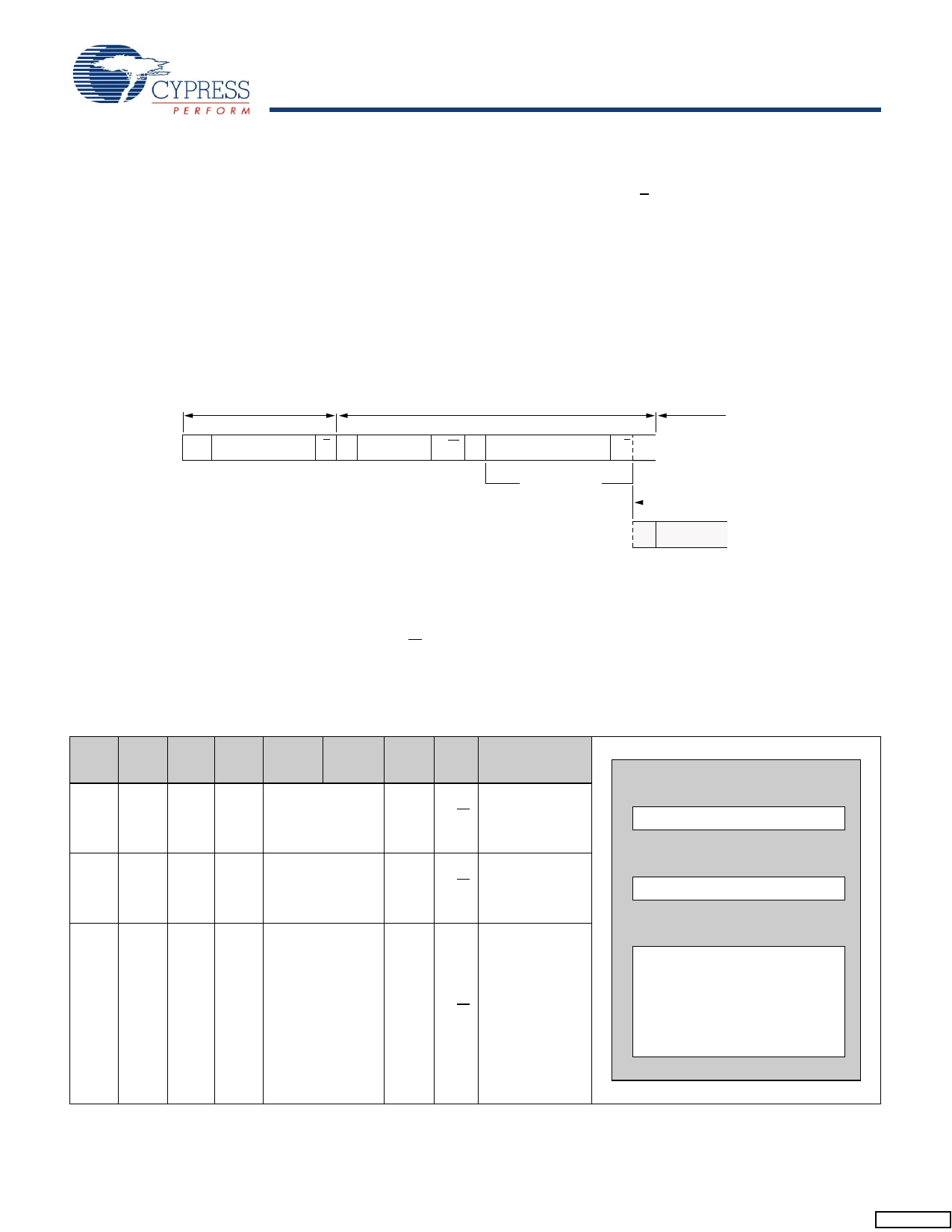
Figure 7. Memory Slave Device Address
handbook, halfpMagSe B
10
LSB
1 0 A2 A1 A16 R/W
Slave ID
Device MSB of
Select Address
RTC Registers Slave Device
The RTC Registers is selected for read/write if the master issues
the slave address as 1101b followed by two bits of device select.
Then, depending on the R/W bit of the slave address, data is
either read from (R/W = вҖҳ1вҖҷ) or written to (R/W = вҖҳ0вҖҷ) the RTC
Registers. The RTC Registers slave address is followed by one
byte address of RTC Register for read/write operation. The RTC
Registers map is explained in the Table 10.
Figure 8. RTC Registers Slave Device Address
handbook, halfpMagSe B
LSB
1 1 0 1 A2 A1 X R/W
Slave ID
Device
Select
Control Registers Slave Device
The Control Registers Slave device includes the serial number,
product ID, Memory Control, and Command Register.
The nvSRAM Control Register Slave device is selected for
read/write if the master issues the slave address as 0011b
followed by two bits of device select. Then, depending on the
R/W bit of the slave address, data is either read from (R/W = вҖҳ1вҖҷ)
or written to (R/W = вҖҳ0вҖҷ) the device.
Document Number: 001-54391 Rev. *G
Page 7 of 41
Share Link: