CXK5V8512TM Ver la hoja de datos (PDF) - Sony Semiconductor
Número de pieza
componentes Descripción
Fabricante
CXK5V8512TM Datasheet PDF : 10 Pages
| |||
CXK5V8512TM
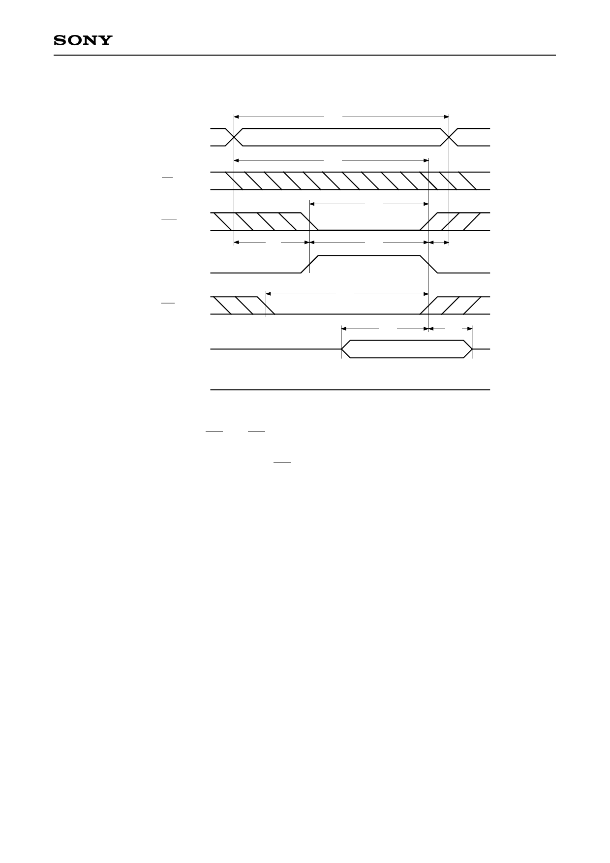
• Write cycle (3) : CE2 control
Address
OE
CE1
CE2
WE
Data in
tWC
tAW
tCW
tAS
tCW
tWR1 (∗3)
tWP
tDW
tDH
Data valid
Data out
High impedance
∗1 Write is executed when both CE1 and WE are at low and CE2 is at high simultaneously.
∗2 Do not apply the data input voltage of the opposite phase to the output while I/O pin is in output condition.
∗3 tWR1 is tested from either the rising edge of CE1 or the falling edge of CE2, whichever comes earlier, until
the end of the write cycle.
–8–
Share Link: 