CXK58512M Ver la hoja de datos (PDF) - Sony Semiconductor
NГәmero de pieza
componentes DescripciГіn
Fabricante
CXK58512M Datasheet PDF : 12 Pages
| |||
CXK58512TM/M
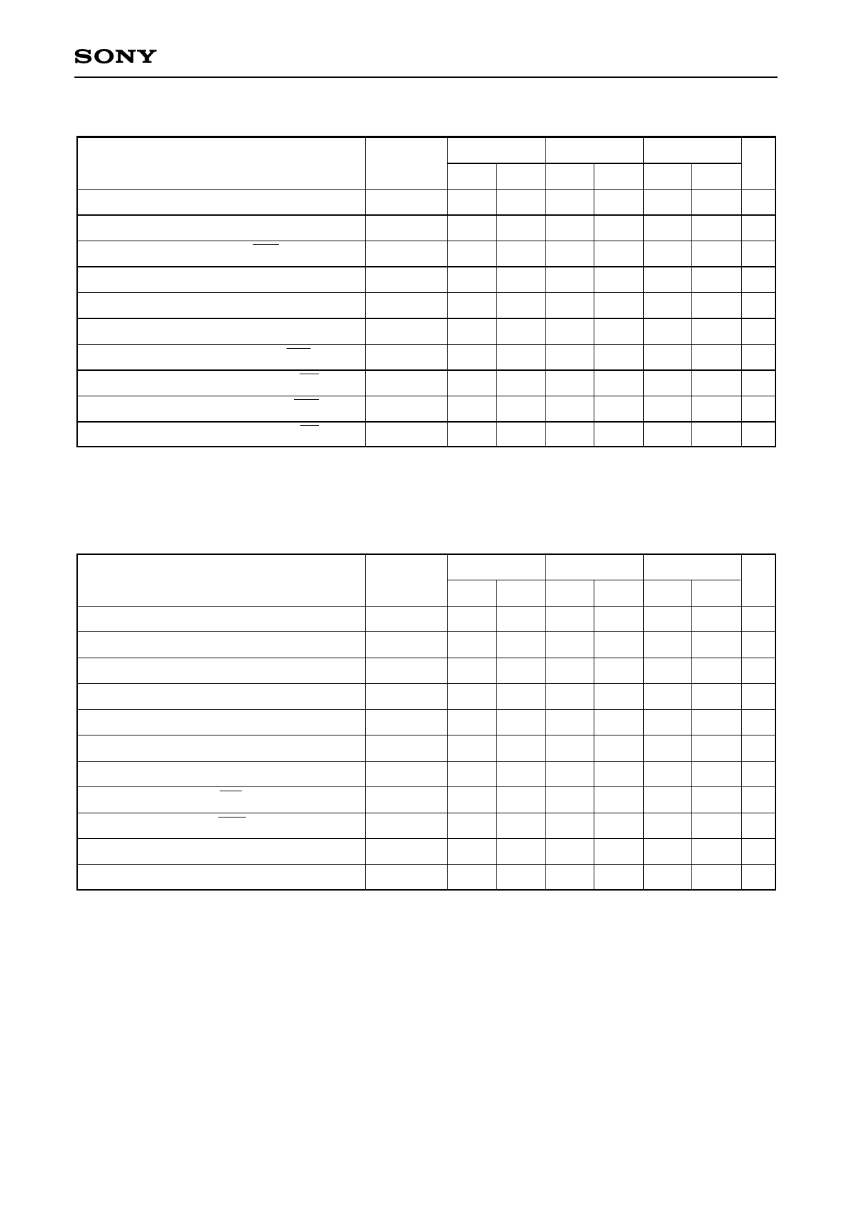
вҖў Read cycle (WE = "H")
(Vcc = 5V Вұ 10%, GND = 0V, Ta = 0 to +70В°C)
-55LL
-70LL
-10LL
Item
Symbol
Unit
Min. Max. Min. Max. Min. Max.
Read cycle time
tRC
55 вҖ” 70 вҖ” 100 вҖ” ns
Address access time
tAA
вҖ” 55 вҖ” 70 вҖ” 100 ns
Chip enable access time (CE1)
tCO1
вҖ” 55 вҖ” 70 вҖ” 100 ns
Chip enable access time (CE2)
tCO2
вҖ” 55 вҖ” 70 вҖ” 100 ns
Output enable to output valid
tOE
вҖ” 30 вҖ” 40 вҖ” 50 ns
Output hold from address change
tOH
15 вҖ” 15 вҖ” 15 вҖ” ns
Chip enable to output in low Z (CE1, CE2) tLZ1, tLZ2
10 вҖ” 10 вҖ” 10 вҖ” ns
Output enable to output in low Z (OE)
tOLZ
5
вҖ”
5вҖ”
5 вҖ” ns
Chip disable to output in high Z (CE1, CE2) tHZ1вҲ—, tHZ2вҲ— вҖ”
25
вҖ” 25
вҖ” 35 ns
Output disable to output in high Z (OE)
tOHZвҲ—
вҖ” 25 вҖ” 25 вҖ” 35 ns
вҲ— tHZ1, tHZ2 and tOHZ are defined as the time required for outputs to turn to high impedance state and are not
referred to as output voltage levels.
вҖў Write cycle
(Vcc = 5V Вұ 10%, GND = 0V, Ta = 0 to +70В°C)
-55LL
-70LL
-10LL
Item
Symbol
Unit
Min. Max. Min. Max. Min. Max.
Write cycle time
tWC
55 вҖ” 70 вҖ” 100 вҖ” ns
Address valid to end of write
tAW
50 вҖ” 60 вҖ” 70 вҖ” ns
Chip enable to end of write
tCW
50 вҖ” 60 вҖ” 70 вҖ” ns
Data to write time overlap
tDW
25 вҖ” 30 вҖ” 40 вҖ” ns
Data hold from write time
tDH
0
вҖ”
0вҖ”
0 вҖ” ns
Write pulse width
tWP
40 вҖ” 50 вҖ” 70 вҖ” ns
Address setup time
tAS
0
вҖ”
0вҖ”
0 вҖ” ns
Write recovery time (WE)
tWR
0
вҖ”
0вҖ”
0 вҖ” ns
Write recovery time (CE1, CE2)
tWR1
0
вҖ”
0вҖ”
0 вҖ” ns
Output active from end of write
Write to output in high Z
tOW
tWHZвҲ—
10 вҖ” 10 вҖ” 10 вҖ” ns
вҖ” 25 вҖ” 25 вҖ” 30 ns
вҲ— tWHZ is defined as the time required for outputs to turn to high impedance state and is not referred to as
output voltage level.
вҖ“5вҖ“
Share Link: 