CXD2570 Ver la hoja de datos (PDF) - Intersil
Número de pieza
componentes Descripción
Fabricante
CXD2570 Datasheet PDF : 8 Pages
| |||
HI2570, CXD2570
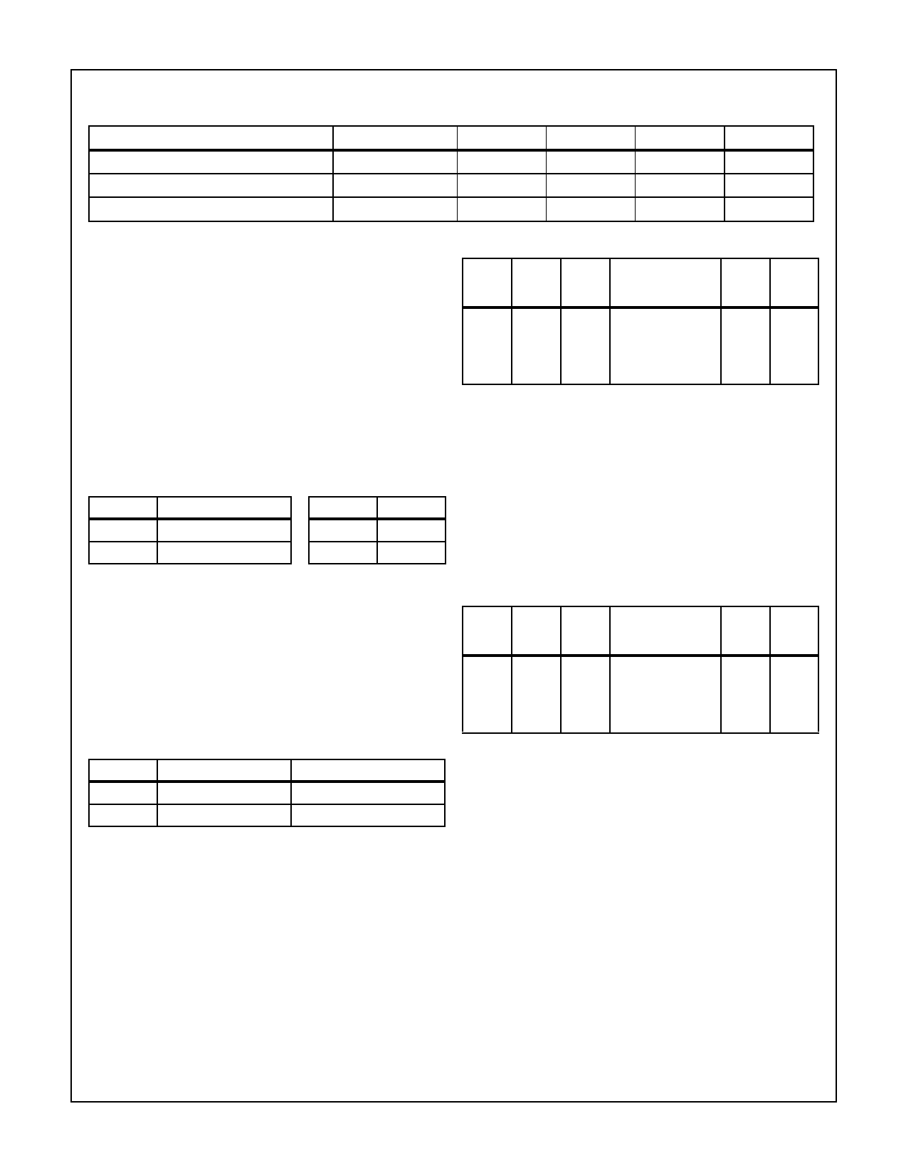
Analog Characteristics AVDD1 = AVDD2 = AVDD3 = AVDD4 = XVDD = DVDD = 5.0V ± 10%, AVSS1 = AVSS2 = AVSS3 = AVSS4 =
XVSS = DVSS = 0V, TA = 25oC (Continued)
ITEM
CONDITIONS
MIN.
TYP.
MAX.
UNIT
Channel Separation
1kHz, 0dB
—
100
—
dB
Gain Difference Between Channels
—
0.05
—
dB
Output Level
RL = 3.9kW
1.80
1.93
2.10
Vrms
Description of Functions
1. Serial data interface
[Related pins] LRCK, BCK, SOUT, SIN, MASL, MLSL
The serial data format is common for both SIN (DA converter
input) and SOUT (AD converter output), consisting of two
channels per sampling serial data represented by 2’s com-
plement. Each channel is divided into 32-bit slots, of which
16 bits are handled as data.
MASL is used to select whether the 16 bits of valid data is
placed in the first or the last half of the 32-bit slots.
Similarly, MLSL is used to select whether the serial data is
arranged at MSB first of LSB first.
MASL
High
Low
Frontward truncation
Rearward truncation
MLSL
High
Low
MSB first
LSB first
2. Master mode/slave mode
[Related pins] MS, LRCK, BCK
When using the CXD2570Q in multiple units or in a pair with
DA converter such as the CXD2558M, one of these
CXD2570Qs should be in the master mode to serve as the
source of clocks LRCK and BCK.
The other ICs including CXD2570Qs are used in the slave
mode, with their clocks LRCK and BCK supplied by the mas-
ter CXD2570Q.
MS
High
Low
MODE
Master mode
Slave mode
LRCK AND BCK I/O
Output
Input
3. Crystal oscillator frequency selection (FS = 16kHz to
48kHz)
[Related pins] XTLI, XTLO, XSL0, XSL1, XSL2, UCLK,
XCLK
By setting a combination of XSL0 and XSL1, with XSL2 fixed
low, the frequency of the external crystal oscillator con-
nected to XTLI and XTLO can be selected. In this case,
XCLK outputs a clock whose frequency is always 256 times
Fs, and UCLK outputs a clock that is half the crystal oscilla-
tor frequency.
When supplying the master clock from some other external
source, not a crystal oscillator, use XTLI for this clock input
and leave XTLO open.
XSL2 XSL1 XSL0
CRYSTAL
OSCILLATOR
FREQUENCY
XCLK UCLK
L
L
L
256Fs
256Fs 128Fs
L
L
H
512Fs
256Fs 256Fs
L
H
L
768Fs
256Fs 384Fs
L
H
H
1024Fs
256Fs 512Fs
*The CXD2555Q, which has the same pin configuration with
this IC is recommended when using only Fs = 32kHz to
48kHz.
4. Crystal oscillator frequency selection (FS = 8kHz to
16kHz)
[Related pins] XTLI, XTLO, XSL0, XSL1, XSL2, UCLK,
XCLK
With XSL2 fixed High, the device can be operated with low-
Fs frequencies. In this case, the frequency of the crystal
oscillator can be selected by setting a combination of XSL0
and XSL1 accordingly.
XSL2
H
H
H
H
XSL1
L
L
H
H
XSL0
L
H
L
H
CRYSTAL
OSCILLATOR
FREQUENCY*
512Fs
—
1024Fs
—
XCLK
512Fs
—
512Fs
—
UCLK
256Fs
—
512Fs
—
5. A/D converter input level
Any desired input level VIN (m . 0.1Vrms) can be selected by
adjusting RIN to generate the full-scale output of the AD con-
verter.
VIN generation of full-scale output varies with the products,
and calculate the VIN maximum level (approximately -3dB
below the full-scale) using the following equation to input the
signal.
(1) Fs = 16kHz to 48kHz (XSL2 = Low)
RIN = 1230 ⋅ VIN [Vrms] -1200 (Ω)
(2) Fs = 8 to 16kHz (XSL2 = High)
RIN = 26600 ⋅ VIN [Vrms] -1200 (Ω)
6. D/A converter output level
To change the D/A converter output level, adjust R15, R17,
R30 and R32 in Application Circuit on page.
7
Share Link: 