CXD2570 Ver la hoja de datos (PDF) - Intersil
Número de pieza
componentes Descripción
Fabricante
CXD2570 Datasheet PDF : 8 Pages
| |||
HI2570, CXD2570
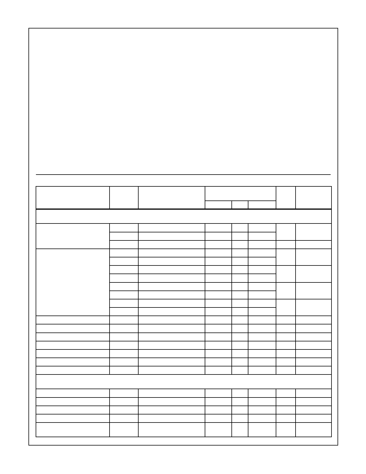
Absolute Maximum Ratings TA = 25oC
Supply Voltage (VDD). . . . . . . . . . . . . . . . . . . . . . VSS–0.5V to 7.0V
Input Voltage (V1). . . . . . . . . . . . . . . . . . .VSS – 0.5V to VDD + 0.5V
Output Voltage (V0) . . . . . . . .
Operating Temperature (Topr)
.
.
.
.
.
.
.
.
.
.
.
.
.
.
.
.
. VSS –
......
0.5V
....
-t2o0VoDCDto+705.5οCV
Storage Temperature (Tstg . . . . . . . . . . . . . . . . . . . -55oC to 150oC
I/O Capacitance
. . . . . . . . . . . . . . . . . . . . . . . . . . . . . . . . . . MIN TYP
Input Pin (CIN)
.—
—
Output Pin (COUT) . . . . . . . . . . . . . . . . . . . —
—
Bidirectional Pin (CI/O) . . . . . . . . . . . . . . . . -— —
Measurement conditions: VDD = V1 = 0V, f = 1MHz
MAX
9pF
11pF
11 pF
Recommended Operating Conditions
. . . . . . . . . . . . . . . . . . . . . . . . . . . . . . . . . . . MIN
Supply Voltage (Note 1) (VDD)
Ambient Temperature (TA) . . .
.
.
.
.
.
.
.
.
.
.
.
4.5V
-20oC
Sampling Frequency (Note 2) (FS). . . . . . . . 7kHz
TYP
5.0V
—
—
MAX
5.5V
+75oC
33kHz
CAUTION: Stresses above those listed in “Absolute Maximum Ratings” may cause permanent damage to the device. This is a stress only rating and operation
of the device at these or any other conditions above those indicated in the operational sections of this specification is not implied.
NOTES:
1. The analog power supplies for AD converters (Pins 17 and 44) must be turned on simultaneously with or before other poser supplies.
turning on these power supplies after any other power supply may cause the device to fall into latch-up condition. this precaution, how-
ever, does not apply when turning off the power supplies.
2. Although the device can operate with FS frequencies such as FS = 44.1kHz or 48kHz, its analog characteristics deteriorate to extent.
When used at only these FS frequencies, the CXD255Q is recommended that is pin-compatible with the CXD2570Q.
Electrical Specifications
PARAMETER
DC Characteristics
Input Voltage
Output Voltage
Input Leak Current 1
Input Leak Current 2
Input Leak Current 3
Input Leak Current 4
Output Leak Current
Feedback Resistance
Supply Current
AC Characteristics
SIN Setup Time
SIN Hold Time
LRCK Setup Time
LRCK Hold Time
LRCK Delay Time
SYMBOL
TEST
CONDITIONS
PART NUMBER
OR GRADE
MIN
TYP
MAX
APPLICABLE
UNITS
PINS
AVDD1
XVSS =
=DAVVSDSD=20=VA, TVADD=3-2=0oACVDtoD745=oCXVDD
=
DVDD
=
5.0V
±
10%,
AVSS1
=
AVSS2
=
AVSS3
=
AVSS4
=
VIHC
0.7VDD —
—
V
*1
VILC
Ò
Ò
0.3VDD
VIN
Analog Input
VSS
—
VDD
V
*2
VOH1
IOH = -2mA
VDD -0.5 —
VDD
V
*3
VOL1
IOL = 4mA
0
—
0.4
VOH2
IOH = -4mA
VDD -0.5 —
VDD
V
*4
VOL2
IOL = 4mA
0
—
0.4
VOH3
IOH = -12mA
VDD/2
—
VDD
V
*5
VOL3
IOL = 16mA
0
—
VDD/2
VOH4
IOH = -2mA
VDD -0.8 —
VDD
V
*6
VOL4
IOL = 4mA
0
—
0.4
ILI1
-10
—
10
µA
*7
ILI2
-40
—
40
µA
*8
ILI3
-20
-50
-12-
µA
*9
ILI4
20
50
120
µA
*10
ILZ
-40
—
40
µA
*11
RFB
VIN = VSS or VDD
250K
1M
‘2.5M
Ω
*12
IDD
(Note 3)
—
43
60
mA
AVDD1 = AVDD2 = AVDD3 = AVDD4 = XVDD = DVDD = 5.0V ± 10%, AVSS1 = AVSS2 = AVSS3 = AVSS4 =
XVSS = DVSS = 0V, TA = -20oC to 75oC
tsus
10
—
—
ns
ths
15
—
—
ns
tsul
Slave mode
10
—
—
ns
thl
Slave mode
15
—
—
ns
tdl
Master mode
CL = 130pF
-40
—
30
ns
5
Share Link: 