CXD2559Q Ver la hoja de datos (PDF) - Intersil
Número de pieza
componentes Descripción
Fabricante
CXD2559Q Datasheet PDF : 11 Pages
| |||
HI2559, CXD2559
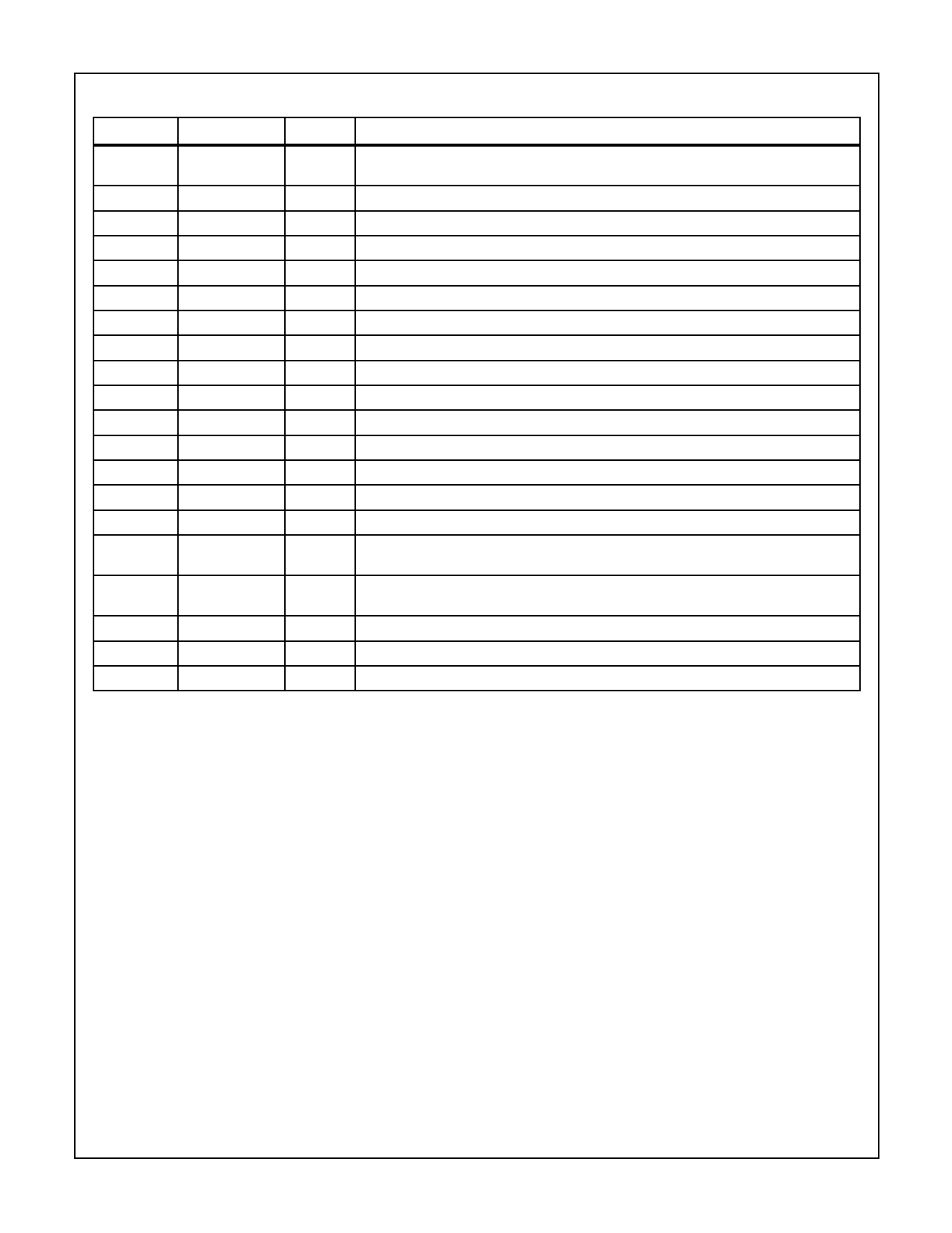
Pin Descriptions (Continued)
PIN NO.
SYMBOL
I/O
13
ATT
I
14
SHIFT
I
15
LATCH
I
16
WO
I
17
DVDD1
-
18
DASL1
I
19
DASL0
I
20
XCLK
O
21
DVSS1
-
22
AVSS1
-
23
AOUT1 (-)
O
24
AVDD1
I
25
AOUT1 (+)
O
26
AVSS2
-
27
XVDD
-
28
XTLO
O
29
XTLI
I
30
XVSS
-
31
AVSS3
-
32
AOUT2 (+)
O
DESCRIPTION
Data input of the microcomputer interface. Attenuation data, output selection setting value,
and de-emphasis on/off data re-input in serial mode.
Shift clock input of the microcomputer interface.
Latch input of the microcomputer interface. Latched at the rising edge.
Synchronization window control. Window open when Low (forced synchronization).
Digital power supply.
IC measurement. Fixed to Low.
IC measurement. Fixed High.
Inversion output of the clock input from XTLI (Pin 1).
Digital GND.
Analog GND for Channel 1 output.
Analog reversed phase output for Channel 1.
Analog power supply for Channel 1 output.
Analog positive phase output for Channel 1.
Analog GND for Channel 1 output.
Digital power supply for the master clock.
Crystal oscillator output. Connects the master clock 256 FS or 384 FS crystal oscillator,
which is identified automatically.
Crystal oscillator input. Connects the master clock 256 FS or 384 FS crystal oscillator,
which is identified automatically. External clock pulse is input at this pin.
Digital GND for master clock
Analog GND for Channel 2 output.
Analog positive phase output for Channel 2.
4-3
Share Link: 