CXD2559Q Ver la hoja de datos (PDF) - Intersil
Número de pieza
componentes Descripción
Fabricante
CXD2559Q Datasheet PDF : 11 Pages
| |||
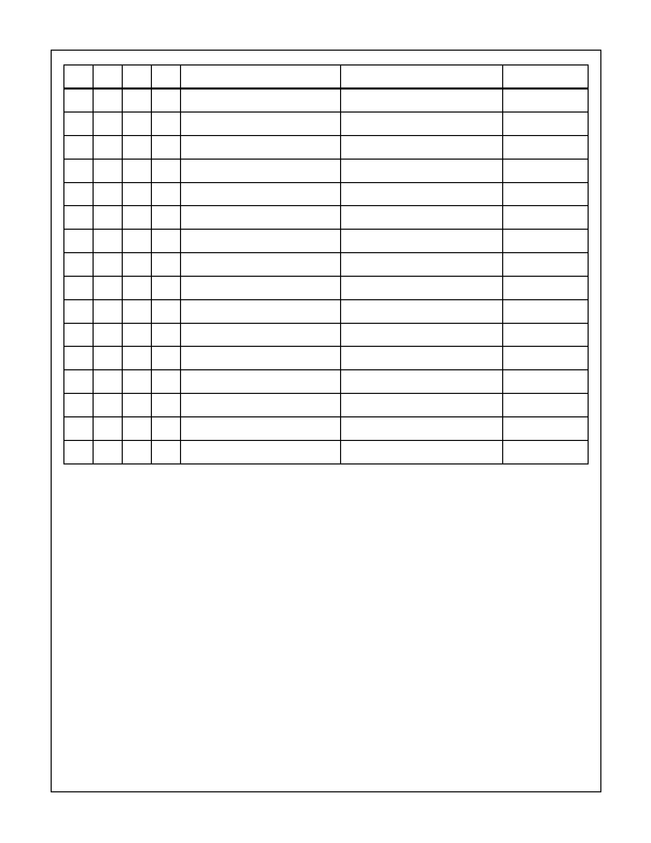
HI2559, CXD2559
P0 P1 P2 P3
L CHANNEL OUTPUT
R CHANNEL OUTPUT
REMARKS
0
0
0
0
Mute
Mute
Mute
0
0
0
1
Mute
R
0
0
1
0
Mute
L
0
0
1
1
Mute
L+R
0
1
0
0
R
Mute
0
1
0
1
R
R
0
1
1
0
R
L
Reverse
0
1
1
1
R
L+R
1
0
0
0
L
Mute
1
0
0
1
L
R
Stereo
1
0
1
0
L
L
1
-
1
1
L
L+R
1
1
0
0
L+R
Mute
1
1
0
1
L+R
R
1
1
1
0
L+R
L
1
1
1
1
L+R
L+R
Mono
NOTE: For L + R, the output data is (L + R)/2 to avoid overflow.
G. I/O Sync Circuit
[Related pins] LRCK and WO
(1) Operation (When the WO Pin is “H”)
The synchronization circuit has the window of eight
clocks of the master clock and it monitors whether the
rising edge of LRCK is in the window.
If the rising edge of LRCK is out of the window, resyn-
chronization is automatically performed.
(2) Forced Synchronization by WO Pin
Even if the rising edge of LRCK is within the window, it
may not synchronize owing to the mixing of the exter-
nal noises, etc. when the rising edge of LRCK is posi-
tioned near at both edges of the window.
When the power is turned on, it is necessary to set the
rising edge of LRCK in the center of the window by
performing the forced synchronization.
After the system is cleared, the forced synchronization
is performed by setting WO pin to Low at 2/FS or
more. The forced synchronization is performed at the
second rising edge of LRCK after the WO pin is turned
to “Low.”
NOTE: WO pin must be “H” except the forced synchronization.
H. System Clear When the Power is Turned ON.
[Related Pins] CLR
When the power is turned ON and the master clock more
than 4 clocks is input to the XTLI pin, set the CLR pin from
“L” to “H.”
4-10
Share Link: 