CXD2598Q Ver la hoja de datos (PDF) - Sony Semiconductor
Número de pieza
componentes Descripción
Fabricante
CXD2598Q Datasheet PDF : 147 Pages
| |||
CXD2598Q
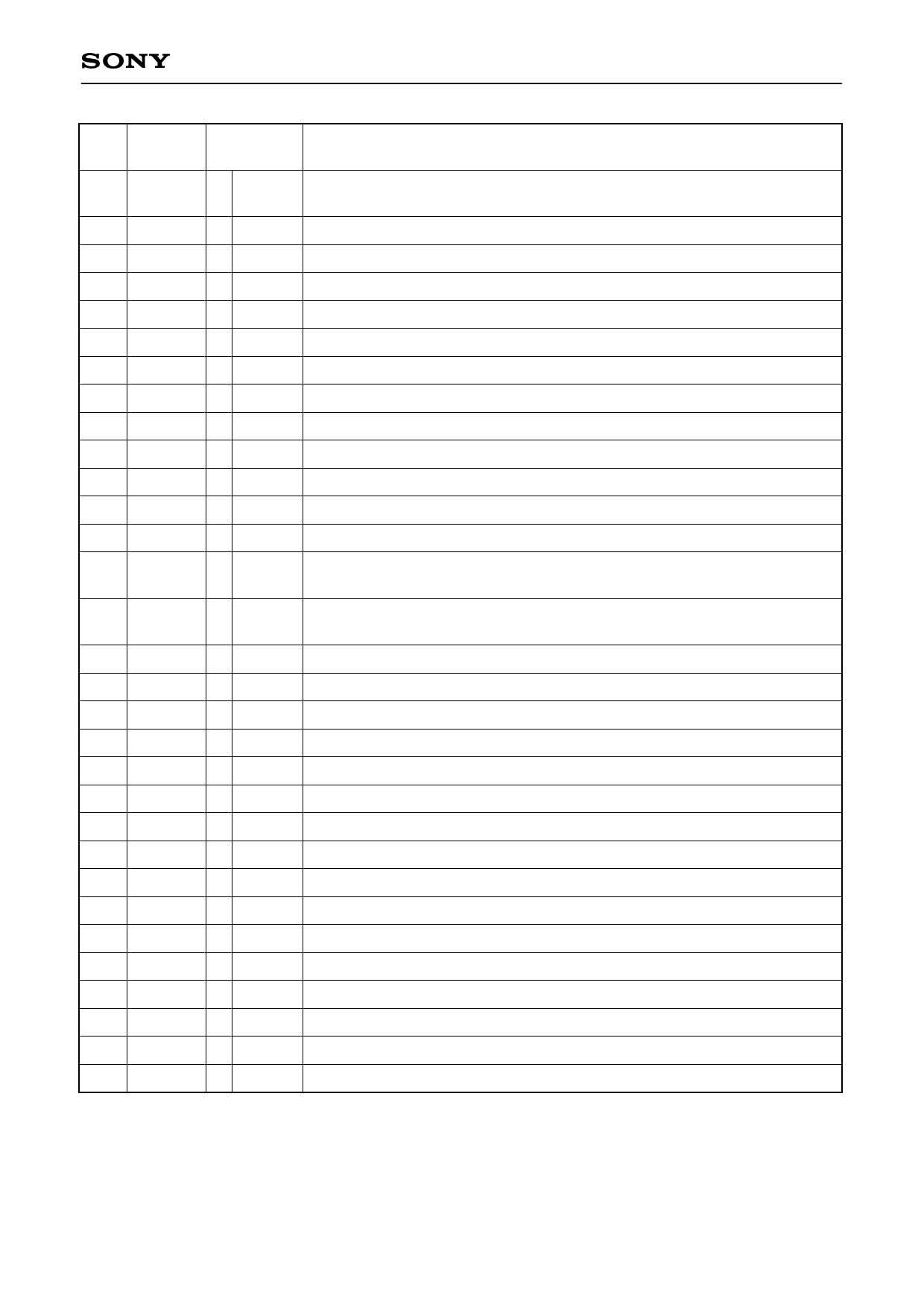
Pin Symbol
I/O
No.
70 V16M I/O 1, 0
71 VPCO O 1, Z, 0
72 VSS
——
73 MD2
I
74 DOUT O 1, 0
75 ASYE
I
76 VDD
——
77 LRCK O 1, 0
78 LRCKI I
79 PCMD O 1, 0
80 PCMDI I
81 BCK
O 1, 0
82 BCKI
I
83 EMPH O 1, 0
84 EMPHI I
85 XVDD
86 XTAI
I
87 XTAO O
88 XVSS
89 AVDD1 — —
90 AOUT1 O
91 AIN1
I
92 LOUT1 O
93 AVSS1 — —
94 AVSS2 — —
95 LOUT2 O
96 AIN2
I
97 AOUT2 O
98 AVDD2 — —
99 RMUT O 1, 0
100 LMUT O 1, 0
Description
Wide-band EFM PLL VCO2 oscillation output. Wide-band EFM PLL clock
input by switching with the command.
Wide-band EFM PLL charge pump output.
Digital GND.
Digital Out on/off control (low = off, high = on).
Digital Out output.
Asymmetry circuit on/off (low = off, high = on).
Digital power supply.
D/A interface. LR clock output f = Fs.
D/A interface. LR clock input.
D/A interface. Serial data output. (two's complement, MSB first)
D/A interface. Serial data input. (two's complement, MSB first)
D/A interface. Bit clock output.
D/A interface. Bit clock input.
Outputs a high signal when the playback disc has emphasis, and a low
signal when there is no emphasis.
Inputs a high signal when emphasis is on, and a low signal when emphasis
is off.
Master clock power supply.
Crystal oscillation circuit input. Master clock is externally input from this pin.
Crystal oscillation circuit output.
Master clock GND.
Analog power supply.
Left channel analog output.
Left channel operational amplifier input.
Left channel LINE output.
Analog GND.
Analog GND.
Right channel LINE output.
Right channel operational amplifier input.
Right channel analog output.
Analog power supply.
Right channel zero detection flag.
Left channel zero detection flag.
–6–
Share Link: 