CXD2598Q Ver la hoja de datos (PDF) - Sony Semiconductor
Número de pieza
componentes Descripción
Fabricante
CXD2598Q Datasheet PDF : 147 Pages
| |||
CXD2598Q
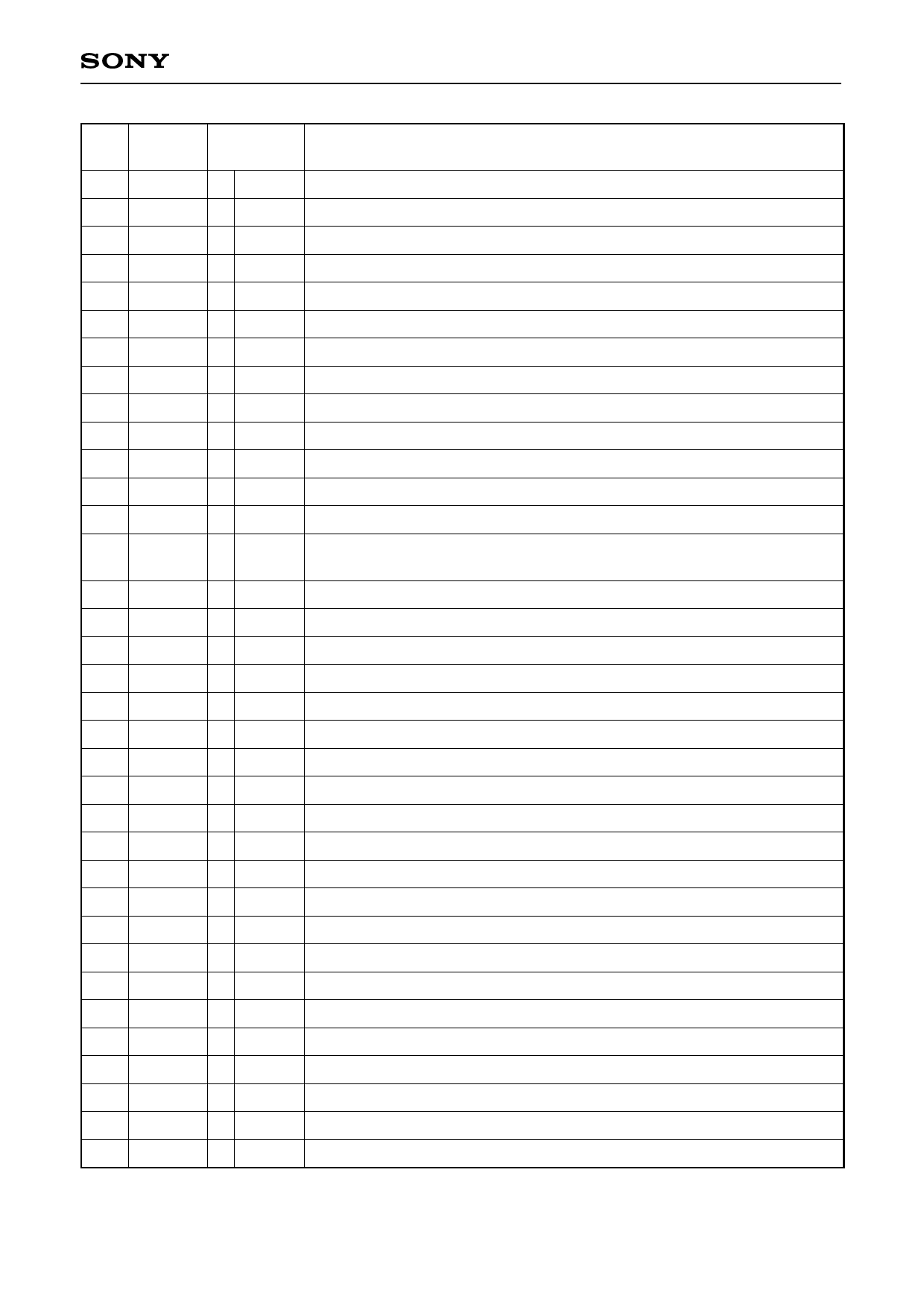
Pin Symbol
I/O
No.
Description
35 MDP
O 1, Z, 0 Spindle motor servo control output.
36 SSTP
I
Disc innermost track detection signal input.
37 FSTIO I/O 1, 0 Input/output of 2/3 frequency division for the XTAI pin.
38 SFDR O 1, 0 Sled drive output.
39 SRDR O 1, 0 Sled drive output.
40 TFDR O 1, 0 Tracking drive output.
41 TRDR O 1, 0 Tracking drive output.
42 FFDR O 1, 0 Focus drive output.
43 FRDR O 1, 0 Focus drive output.
44 VDD
— — Digital power supply.
45 VSS
— — Digital GND.
46 TEST
I
Test pin. Normally, GND.
47 TES1
I
Test pin. Normally, GND.
48 XTSL
I
Crystal selection input. Low when the crystal is 16.9344MHz; high when the
crystal is 33.8688MHz.
49 VC
I
Center voltage input.
50 FE
I
Focus error signal input.
51 SE
I
Sled error signal input.
52 TE
I
Tracking error signal input.
53 CE
I
Center servo analog input.
54 RFDC I
RF signal input.
55 ADIO
O Analog Test pin. Do not connect anything.
56 AVSS0 — — Analog GND.
57 IGEN
I
Operational amplifier constant current input.
58 AVDD0 — — Analog power supply.
59 ASYO O 1, 0 EFM full-swing output (low = VSS, high = VDD).
60 ASYI
I
Asymmetry comparator voltage input.
61 RFAC I
EFM signal input.
62 AVSS3 — —
Analog GND.
63 CLTV
I
Multiplier VCO1 control voltage input.
64 FILO
O Analog Master PLL filter output (slave = digital PLL).
65 FILI
I
Master PLL filter input.
66 PCO
O 1, Z, 0 Master PLL charge pump output.
67 AVDD3 — —
Analog power supply.
68 BIAS
I
Asymmetry circuit constant current input.
69 VCTL
I
Wide-band EFM PLL VCO2 control voltage input.
–5–
Share Link: 