CXA3503 Ver la hoja de datos (PDF) - Sony Semiconductor
Número de pieza
componentes Descripción
Fabricante
CXA3503 Datasheet PDF : 42 Pages
| |||
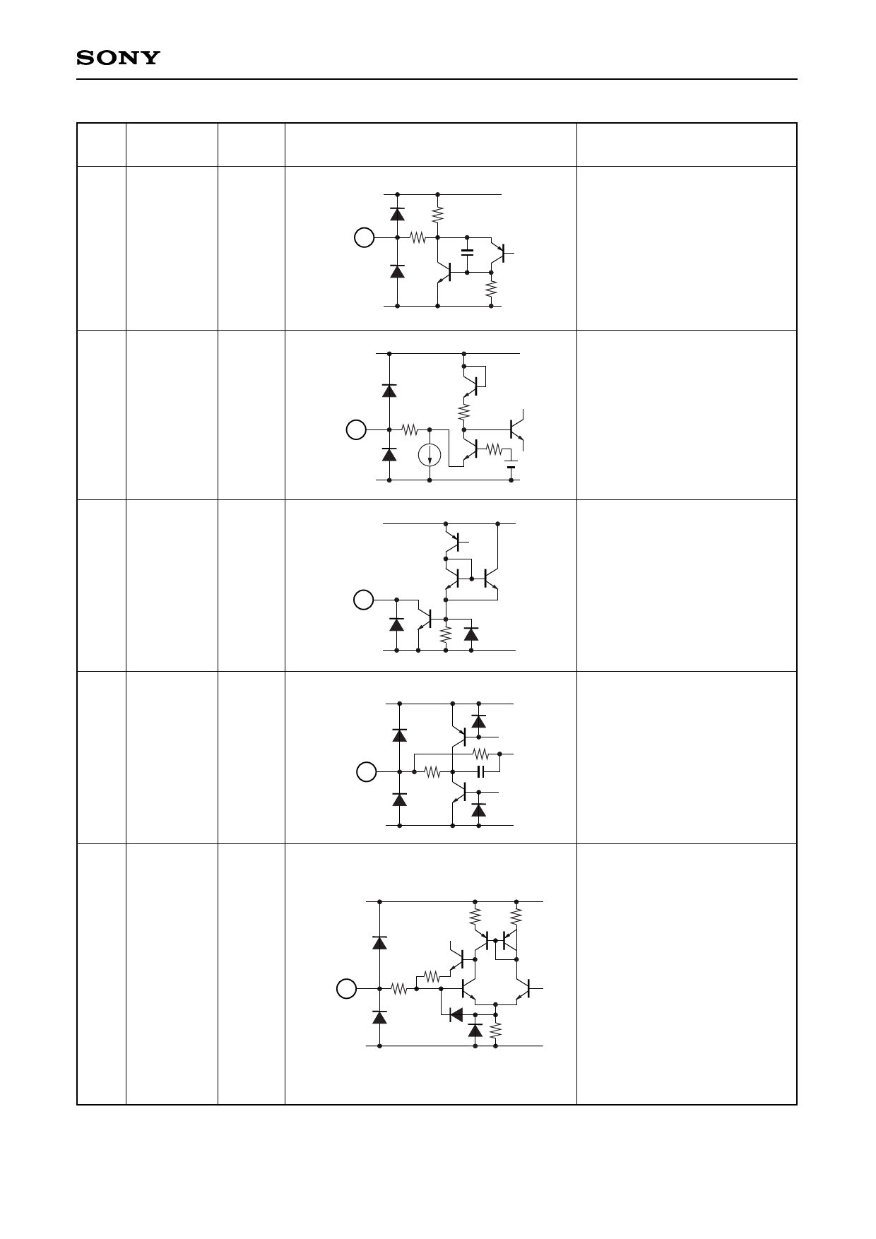
Analog Block Pin Description
Pin
No.
Symbol
Pin
voltage
2 FIL OUT
2.15V
3 SYNC IN
1.1V
4 SYNC OUT —
6 DA OUT
—
Equivalent circuit
VCC1
2
23k
200
GND1
VCC1
200
3
GND1
VCC1
4
GND1
VCC1
6
GND1
50
50
8 F ADJ
1.1V
VCC1
6.5k
8
10
GND1
–5–
CXA3503R
Description
Amplifies and outputs the sync
portion of the video signal input
to FIL IN (Pin 69).
Sync separation circuit input.
Inputs the FIL OUT (Pin 2)
output signal via a capacitor.
Sync separation output.
Positive polarity output in open
collector format.
DA output.
Outputs the serial data
converted to DC voltage. The
current driving capacity is
±1.0mA (max.).
Connect a resistor between this
pin and GND1 to control the
internal LPF and trap
frequencies.
Connect a 33kΩ resistor
(tolerance ±2%, temperature
characteristics ±200ppm or less).
This pin is easily affected by
external noise, so make the
connection between the pin and
external resistor, and between
the GND side of the external
resistor and the GND1 pin as
close as possible.
Share Link: 