CXA3086 Ver la hoja de datos (PDF) - Sony Semiconductor
Número de pieza
componentes Descripción
Fabricante
CXA3086 Datasheet PDF : 30 Pages
| |||
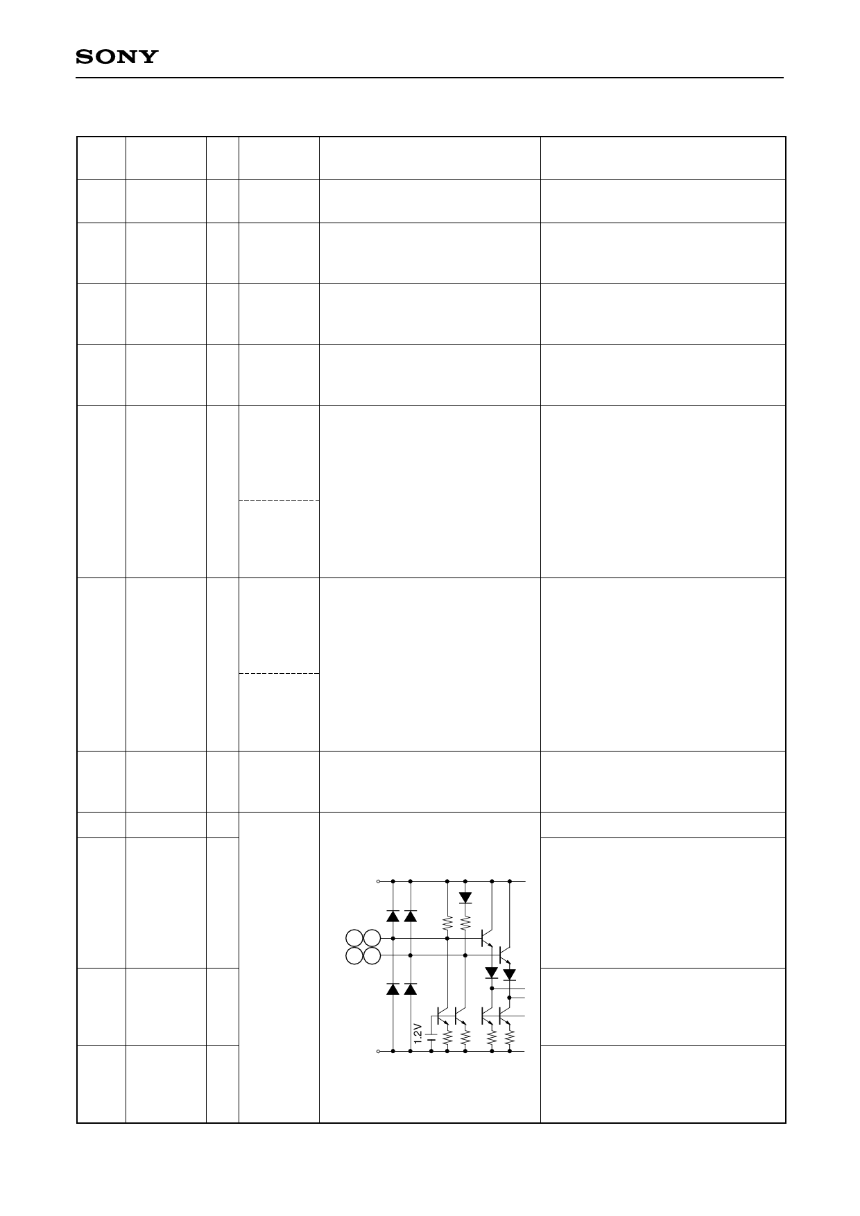
Pin Description and I/O Pin Equivalent Circuit
Pin Symbol I/O Standard
No.
voltage level
Equivalent circuit
14, 23 AGND
GND
17, 20 AVCC
1, 8, DGND1
29, 36, DGND2
39, 46
9, 28,
37, 38,
47, 48
DVCC1
DVCC2
24 DGND3
13 DVEE3
18, 40, N.C.
45
25 CLK/E
+5V
(typ.)
GND
+5V
(typ.)
+5V (typ.)
(With a
single
power
supply)
GND
(With dual
power
supplies)
GND
(With a
single
power
supply)
–5V (typ.)
(With dual
power
supplies)
I
DGND3
26 CLKN/E I
12 25
rr
ECL/
PECL
11 26
12 RESETN/E I
DVEE3
rr
11 RESET/E I
–4–
CXA3086Q
Description
Analog ground.
Separated from the digital ground.
Analog power supply.
Separated from the digital power
supply.
Digital ground.
Digital power supply.
Digital power supply.
Ground for ECL input.
+5V for PECL and TTL input.
Digital power supply.
–5V for ECL input.
Ground for PECL and TTL input.
No connected pin.
Not connected with the internal
circuits.
Clock input.
CLK/E complementary input.
When left open, this pin goes to the
threshold potential.
Only CLK/E can be used for
operation, but complementary input
is recommended to attain fast and
stable operation.
Reset input.
When the input is set to low level,
the built-in CLK frequency divider
circuit can be reset.
RESETN/E complementary input.
When left open, this pin goes to the
threshold voltage. Only RESETN/E
can be used for operation.
Share Link: 