CXA1812Q Ver la hoja de datos (PDF) - Sony Semiconductor
Número de pieza
componentes Descripción
Fabricante
CXA1812Q Datasheet PDF : 22 Pages
| |||
CXA1812Q
∗Externally applied voltage
Pin
Pin
Symbol
No.
voltage
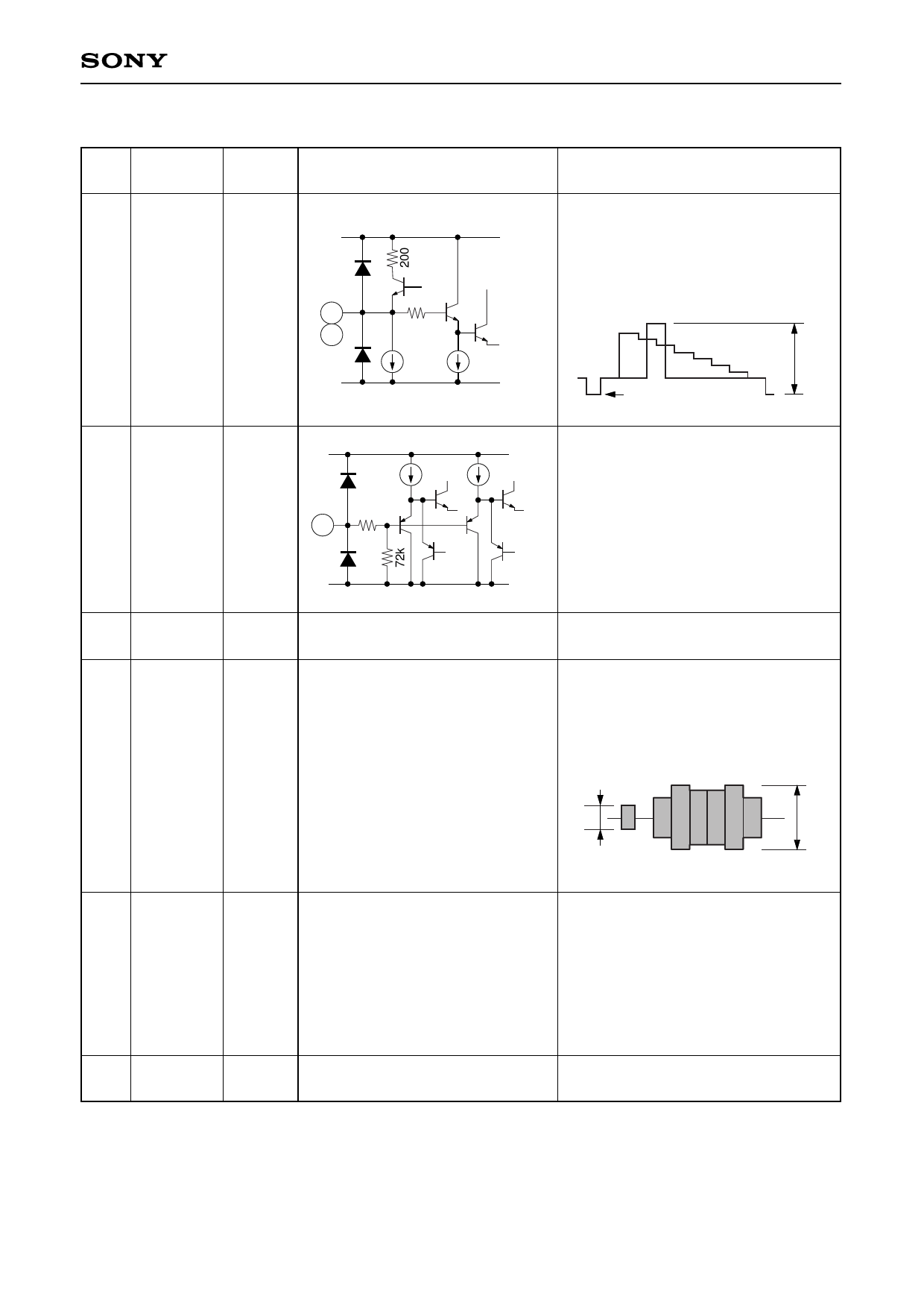
Equivalent circuit
Description
Video input Y signal inputs. Coupled
by means of a capacitor; in order to
VCC
keep clamp error to a minimum, keep
the input impedance as low as
23
YIN1
2.5 V
25
YIN2 (Sync tip) 23
1100
25
possible.
0.5Vp-p
1µ
40µ
GND
2.5V
24 INSEL
26
GND
27
CIN1
29
CIN2
0V
0 V∗
—
VCC Control input for switching between
20µ
20µ
signals input from Pins 23 and 25 and
from Pins 27 and 29.
24
150
Low (0 to 0.8 V) :
signals at Pins 23 and 27 are selected
High (2 V to VCC) :
GND signals at Pins 25 and 29 are selected
—
Same as for Pin 7.
GND other than the 75 Ω driver.
Video input chroma signal inputs.
Coupled by means of a capacitor within
the IC.
Inputting a signal of –0.3 V or less may
lead waveform distortion.
28 Y/VSEL
0V
30 YOUTGND 0 V∗
Same as for Pin 6.
—
143mVp-p
314mVp-p
Control input for switching the output
signal format for Pin 19.
Pin 19 output
Pin 21 output
Low : Y signal
Chroma signal
High : Composite High impedance
video signal
Low (0 to 0.8 V) High (2 V to VCC)
Y 75 Ω driver GND.
—7—
Share Link: 