CXA1810 Ver la hoja de datos (PDF) - Sony Semiconductor
Número de pieza
componentes Descripción
Fabricante
CXA1810 Datasheet PDF : 53 Pages
| |||
CXA1810AQ/AR
Pin
Symbol
No.
30 V IN1
Pin voltage
DC
AC
2.05V
Video
(sync tip
500mVp-p
level)
input
31 REC L/JVD 1.9V
—
(Typical value
during REC
LEVEL
adjustment)
32 Y IN
1.6V
(sync tip
level)
Video
500mVp-p
input
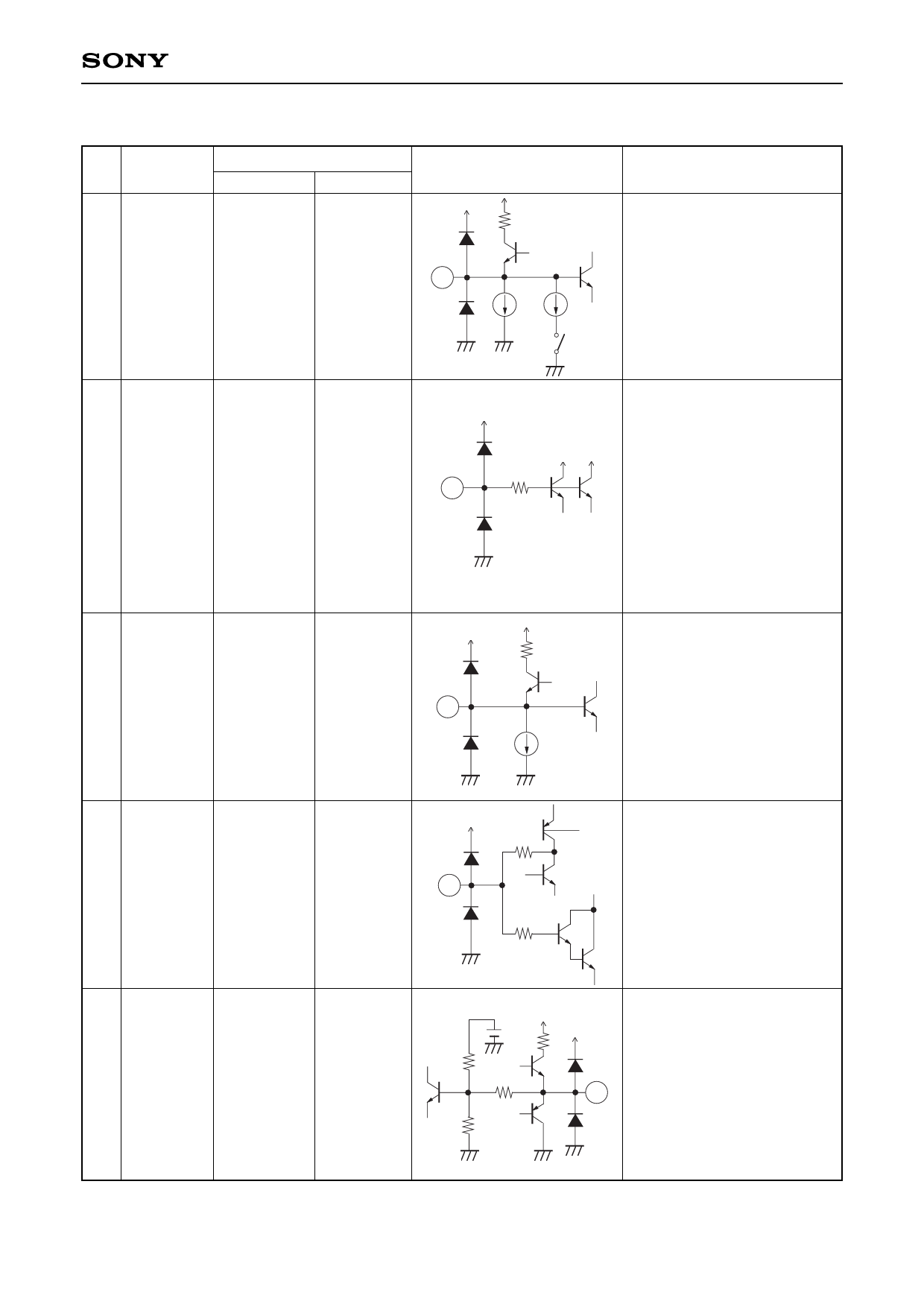
Equivalent circuit
Description
Video signal input. Performs
270
diode clamping, with the
clamp capacitance externally
30
connected. If the mode MUTE
is set High, the charge of the
100nA 4µA
clamp capacitance is
MUTE discharged.
ON
Level adjustment during
recording. The adjustment
range is 1.3V to 2.6V. During
playback, serves as input for
31
150
JOG (variable speed
playback) VD pulse and HD
pulse.
VTH = 2.7V
(Refer to item 3 on Description
of Operation.)
Video signal input for video
270
out circuit. Performs diode
clamping, with the clamp
capacitance externally
32
connected.
100nA
33 CLAMP TC1
—
—
100
33
100
Time constant for feedback
clamp circuit in I/O block.
34 Y OUT
1.8V
(sync tip
level)
Video
500mVp-p
output
2.05V
3.4k
3k
150
34
I/O block signal output.
27k
—10—
Share Link: 