CS5461A Ver la hoja de datos (PDF) - Cirrus Logic
Número de pieza
componentes Descripción
Fabricante
CS5461A Datasheet PDF : 44 Pages
| |||
CS5461A
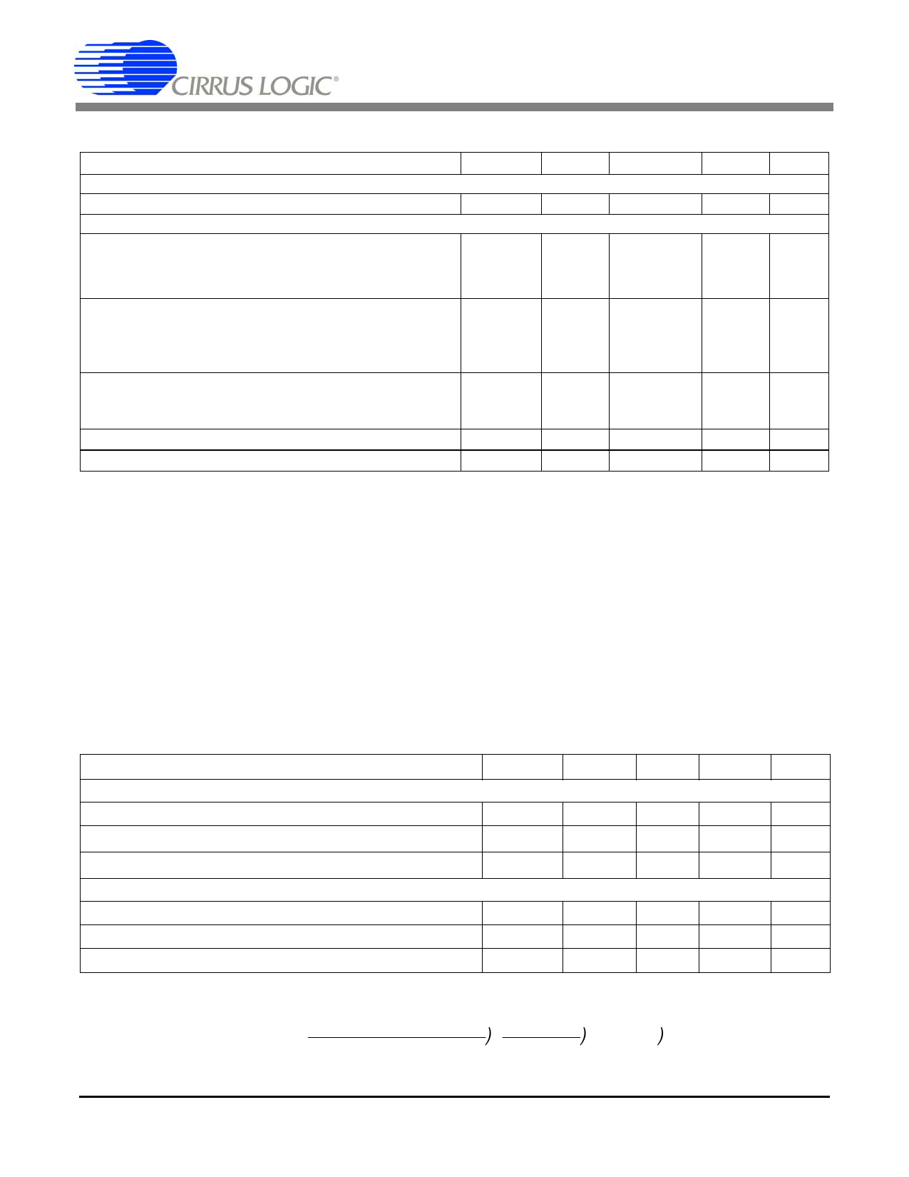
ANALOG CHARACTERISTICS (Continued)
Parameter
Symbol Min
Temperature Channel
Temperature Accuracy
T
-
Power Supplies
Power Supply Currents (Active State)
IA+ PSCA
-
ID+ (VA+ = VD+ = 5 V) PSCD
-
ID+ (VA+ = 5 V, VD+ = 3.3 V) PSCD
-
Power Consumption Active State (VA+ = VD+ = 5 V)
-
(Note 3)
Active State (VA+ = 5 V, VD+ = 3.3 V)
Stand-By State
PC
-
-
Sleep State
-
Power Supply Rejection Ratio
(Note 4)
(DC, 50 and 60 Hz)
Voltage Channel
Current Channel
PSRR
45
70
PFMON Low-voltage Trigger Threshold
(Note 5) PMLO
2.3
PFMON High-voltage Power-On Trip Point
(Note 6) PMHI
-
Typ
±5
1.1
2.9
1.7
21
12
8
10
65
75
2.45
2.55
Max Unit
-
°C
-
mA
-
mA
-
mA
28
mW
16.5 mW
-
mW
-
µW
-
dB
-
dB
-
V
2.7
V
1. Applies when the HPF option is enabled.
2. Applies before system calibration.
3. All outputs unloaded. All inputs CMOS level.
4. Measurement method for PSRR: VREFIN tied to VREFOUT, VA+ = VD+ = 5 V, a 150 mV (zero-to-peak) (60 Hz)
sinewave is imposed onto the +5 V DC supply voltage at VA+ and VD+ pins. The “+” and “-” input pins of both input
channels are shorted to AGND. Then the CS5461A is commanded to continuous conversion acquisition mode, and
digital output data is collected for the channel under test. The (zero-to-peak) value of the digital sinusoidal output
signal is determined, and this value is converted into the (zero-to-peak) value of the sinusoidal voltage (measured
in mV) that would need to be applied at the channel’s inputs, in order to cause the same digital sinusoidal output.
This voltage is then defined as Veq. PSRR is then (in dB):
PSRR
=
20
⋅
log
⎧
⎨
⎩
-1---5---0--
Veq
⎫
⎬
⎭
5. When voltage level on PFMON is sagging, and LSD bit is at 0, the voltage at which LSD bit is set to 1.
6. If the LSD bit has been set to 1 (because PFMON voltage fell below PMLO), this is the voltage level on PFMON at
which the LSD bit can be permanently reset back to 0.
VOLTAGE REFERENCE
Parameter
Reference Output
Output Voltage
Temperature Coefficient
Load Regulation
Reference Input
Input Voltage Range
Input Capacitance
Input CVF Current
Symbol Min
VREFOUT
(Note 7) TCVREF
(Note 8) ∆VR
+2.4
-
-
VREFIN
+2.4
-
-
Typ
+2.5
25
6
+2.5
4
25
Max Unit
+2.6
60
10
V
ppm/°C
mV
+2.6
V
-
pF
-
nA
Notes: 7. The voltage at VREFOUT is measured across the temperature range. From these measurements the following
formula is used to calculate the VREFOUT Temperature Coefficient:.
( ( T C V R E F =
(V R E F O U T M A X - V R E F O U T M IN )
V R E FO U TAVG
1
T A M A X - T A M IN
8. Specified at maximum recommended output of 1 µA, source or sink.
( 1 .0 x 1 0 6
8
DS661F2
Share Link: 