CS52015-3GST3 Ver la hoja de datos (PDF) - ON Semiconductor
Número de pieza
componentes Descripción
Fabricante
CS52015-3GST3 Datasheet PDF : 8 Pages
| |||
CS52015−3
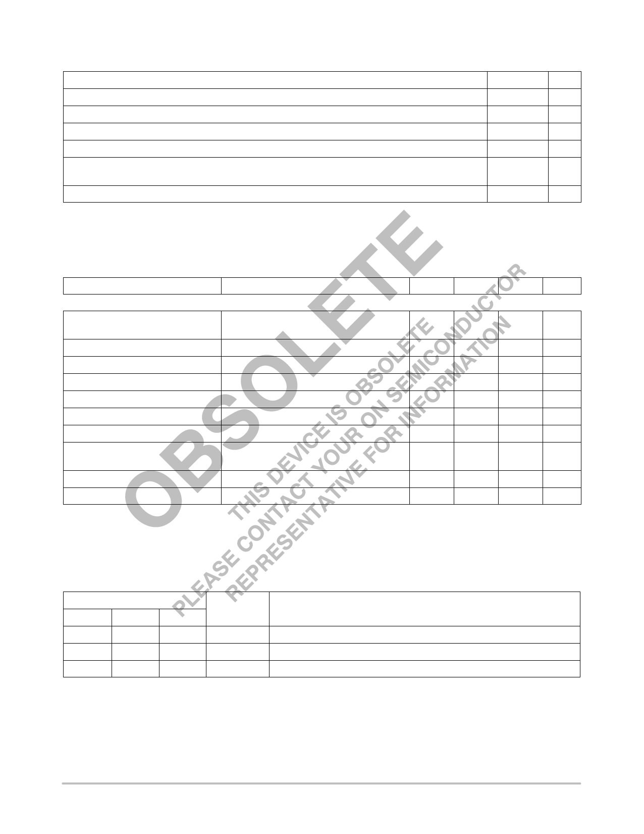
MAXIMUM RATINGS*
Parameter
Value
Unit
Supply Voltage, VIN
Operating Temperature Range
Junction Temperature
Storage Temperature Range
7.0
V
−40 to +70
°C
150
°C
−60 to +150 °C
Lead Temperature Soldering:
Wave Solder (through hole styles only) Note 1 260 Peak
°C
Reflow (SMD styles only) Note 2 230 Peak
°C
ESD Damage Threshold
1. 10 second maximum.
2. 60 second maximum above 183°C
*The maximum package power dissipation must be observed.
2.0
kV
ELECTRICAL CHARACTERISTICS (CIN = 10 mF, COUT = 22 mF Tantalum, VOUT + VDROPOUT < VIN < 7.0 V, 0°C ≤ TA ≤ 70°C,
TJ ≤ +150°C, unless otherwise specified, Ifull load = 1.5 A)
Characteristic
Test Conditions
Min
Typ
Max
Unit
Fixed Output Voltage
Output Voltage (Notes 3 and 4)
Line Regulation
Load Regulation (Notes 3 and 4)
Dropout Voltage (Note 5)
Current Limit
Quiescent Current
Thermal Regulation (Note 6)
Ripple Rejection (Note 6)
Thermal Shutdown (Note 7)
VIN − VOUT = 1.5 V;
0 ≤ IOUT ≤ 1.5 A
2.0 V ≤ VIN − VOUT ≤ 3.7 V; IOUT = 10 mA
VIN − VOUT = 2.0 V; 10 mA ≤ IOUT ≤ 1.5 A
IOUT = 1.5 A
VIN − VOUT = 3.0 V
IOUT = 10 mA
30 ms Pulse, TA = 25°C
f = 120 Hz; IOUT = 1.5 A; VIN − VOUT = 3.0 V;
VRIPPLE = 1.0 VPP
−
3.250
(−1.5%)
−
−
−
1.6
−
−
−
3.300
0.02
0.04
1.05
3.1
5.0
0.002
80
3.350
(+1.5%)
0.20
0.4
1.4
−
10
0.020
−
V
%
%
V
A
mA
%/W
dB
150
180
210
°C
Thermal Shutdown Hysteresis (Note 7)
−
−
25
−
°C
3. Load regulation and output voltage are measured at a constant junction temperature by low duty cycle pulse testing. Changes in output
voltage due to temperature changes must be taken into account separately.
4. Specifications apply for an external Kelvin sense connection at a point on the output pin 1/4” from the bottom of the package.
5. Dropout voltage is a measurement of the minimum input/output differential at full load.
6. Guaranteed by design, not 100% tested in production.
7. Thermal shutdown is 100% functionally tested in production.
PACKAGE PIN DESCRIPTION
Package Pin Number
TO−220−3 D2PAK−3 SOT−223
1
1
1
2
2
2
3
3
3
Pin Symbol
GND
VOUT
VIN
Ground connection.
Regulated output voltage (case).
Input voltage.
Function
http://onsemi.com
2
Share Link: 