CS2842A Ver la hoja de datos (PDF) - Cherry semiconductor
Número de pieza
componentes Descripción
Fabricante
CS2842A Datasheet PDF : 6 Pages
| |||
Circuit Description: continued
former saturation in some power supplies, the internal
oscillator waveform provides the maximum duty cycle
clamp as programmed by the selection of oscillator com-
VOSC
ponents.
OSC
RESET
EA Output
Switch
Current
VCC
IOUT
VOUT
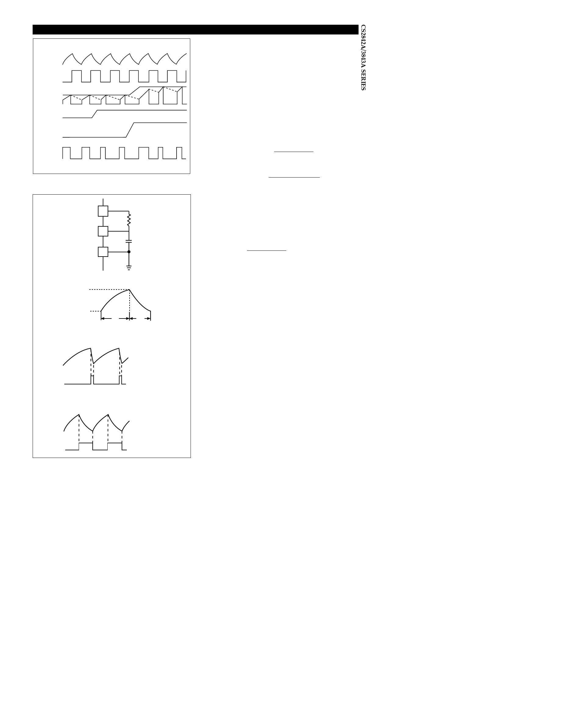
Setting the Oscillator
Oscillator timing capacitor, CT, is charged by VREF through
RT and discharged by an internal current source. During
the discharge time, the internal clock signal blanks out the
output to the Low state, thus providing a user selected
maximum duty cycle clamp. Charge and discharge times
are determined by the formula:
( ) tc = RTCT ln
VREF - Vlower
VREF - Vupper
Figure 2: Timing Diagram for key CS2841B parameters
( ) td = RTCT ln
VREF - IdRT - Vlower
VREF - IdRT - Vupper
VREF
RT
OSC
CT
Gnd
Timing parameters
Vupper
Vlower
tc
Sawtooth Mode
LARGE RT (≈10kΩ)
td
VOSC
Substituting in typical values for the parameters in the
above formulas:
VREF = 5.0V, Vupper = 2.7V, Vlower = 1.0V, Id = 8.3mA
tc ≈ 0.5534RTCT
( ) td = RTCT ln
2.3 - 0.0083 RT
4.0 - 0.0083 RT
The frequency and maximum duty cycle can be deter-
mined using the Typical Performance Characteristic
graphs.
Grounding
High peak currents associated with capacitive loads neces-
sitate careful grounding techniques. Timing and bypass
capacitors should be connected close to Gnd pin in a sin-
gle point ground.
The transistor and 5kΩ potentiometer, shown in the test
circuit, are used to sample the oscillator waveform and
apply an adjustable ramp to Sense.
Triangular Mode
SMALL RT (≈700kΩ)
Internal Clock
VREF
Internal Clock
Figure 3: Oscillator Timing Network and parameters
5
Share Link: 