CPC5602(2008) Ver la hoja de datos (PDF) - Clare Inc => IXYS
Número de pieza
componentes Descripción
Fabricante
CPC5602 Datasheet PDF : 3 Pages
| |||
CPC5602
N Channel Depletion Mode FET
Parameter
Drain-to-Source Voltage (VDS)
Max On-Resistance (Ron-max)
Max Power
Rating
350
14
2.5
Units
V
Ω
W
Features
• 350V Drain-to-Source Voltage
• Low On-resistance: 8 Ohms (Typical)
• High input impedance
• Low input and output leakage
• Small package size SOT-223
• PC Card (PCMCIA) Compatible
• PCB Space and Cost Savings
Applications
• Support Component for LITELINK™
Data Access Arrangement (DAA)
• Telecommunications
Description
The CPC5602 is an “N” channel depletion mode Field
Effect Transistor (FET) that utilizes Clare’s proprietary
third generation vertical DMOS process. The third
generation process realizes world class, high voltage
MOSFET performance in an economical silicon gate
process. The vertical DMOS process yields a highly
reliable device, particularly in difficult application
environments such as telecommunications.
One of the primary applications for the CPC5602 is
as a linear regulator/hook switch for the LITELINK
family of Data Access Arrangements (DAA) Devices
CPC5610A, CPC5611A, CPC5620A, CPC5621A,
and CPC5622A.
The CPC5602 has a typical on-resistance of 8Ω, a
drain-to-source voltage of 350V, and is available in
an SOT-223 package. As with all MOS devices, the
FET structure prevents thermal runaway and thermal-
induced secondary breakdown.
Ordering Information
Part Number
CPC5602C
CPC5602CTR
Description
N-Channel Depletion Mode FET, SOT-223
Package (80/tube)
N-Channel Depletion Mode FET, SOT-223
Package Tape and Reel (1000/reel)
Pb
RoHS
2002/95/EC
DS-CPC5602-R05
e3
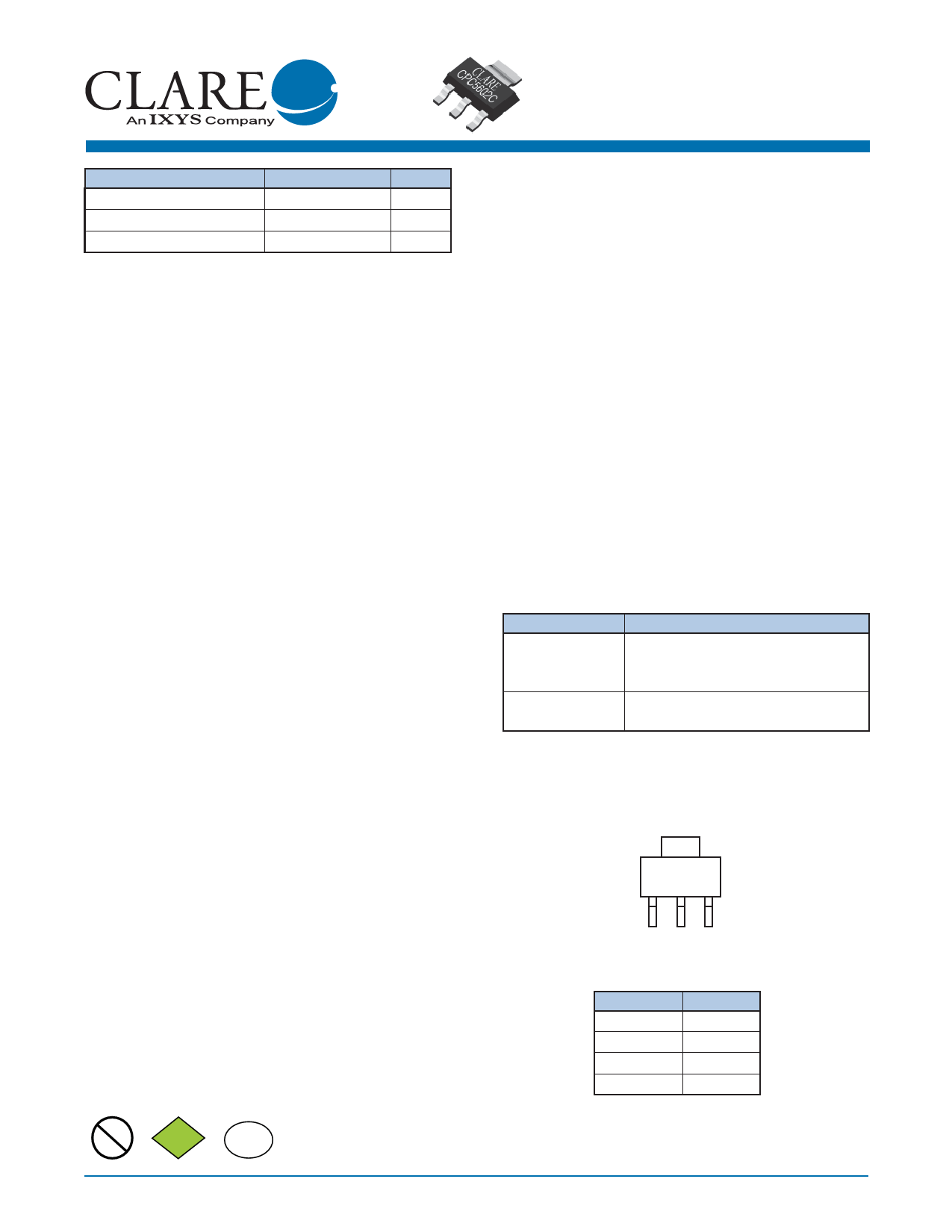
Package Pinout
D
4
123
GDS
Pin Number
1
2
3
4
Name
GATE
DRAIN
SOURCE
DRAIN
www.clare.com
1
Share Link: 