LTC1265I Ver la hoja de datos (PDF) - Linear Technology
Número de pieza
componentes Descripción
Fabricante
LTC1265I Datasheet PDF : 16 Pages
| |||
LTC1265/LTC1265-3.3/LTC1265-5
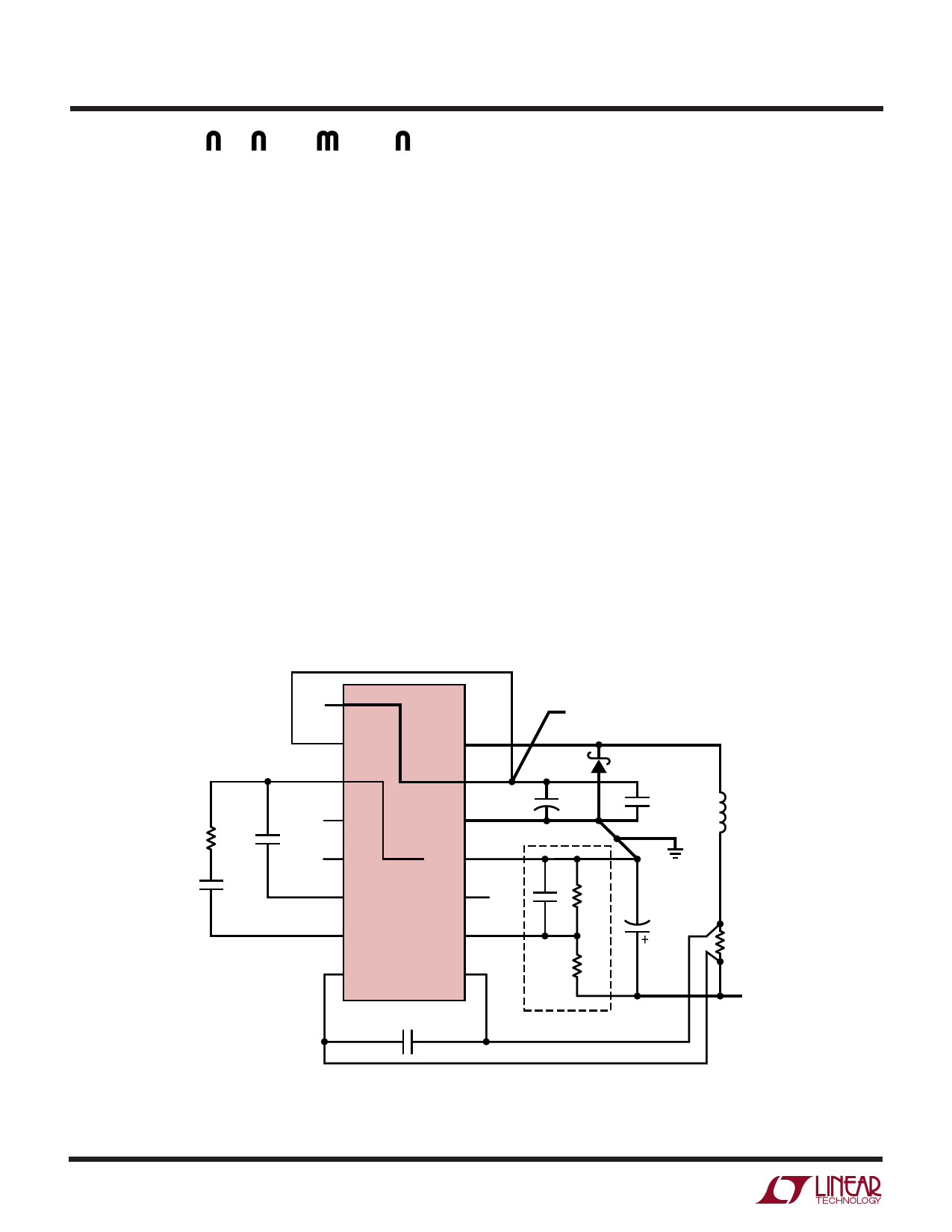
APPLICATIONS INFORMATION
Board Layout Checklist
When laying out the printed circuit board, the following
checklist should be used to ensure proper operation of the
LTC1265. These items are also illustrated graphically in
the layout diagram of Figure 5. Check the following in your
layout:
1. Are the signal and power grounds segregated? The
LTC1265 signal ground (Pin 11) must return to the (–)
plate of COUT. The power ground (Pin 12) returns to the
anode of the Schottky diode, and the (–) plate of CIN,
whose leads should be as short as possible.
2. Does the (+) plate of the CIN connect to the power VIN
(Pins 1,13) as close as possible? This capacitor pro-
vides the AC current to the internal P-channel MOSFET
and its driver.
3. Is the input decoupling capacitor (0.1µF) connected
closely between power VIN (Pins 1,13) and power
ground (Pin 12)? This capacitor carries the high fre-
quency peak currents.
4. Is the Schottky diode closely connected between the
power ground (Pin 12) and switch (Pin 14)?
5. Does the LTC1265 SENSE– (Pin 7) connect to a point
close to RSENSE and the (+) plate of COUT? In adjustable
applications, the resistive divider, R1 and R2, must be
connected between the (+) plate of COUT and signal
ground.
6. Are the SENSE– and SENSE+ leads routed together with
minimum PC trace spacing? The 1000pF capacitor
between Pins 7 and 8 should be as close as possible to
the LTC1265.
7. Is SHDN (Pin 10) actively pulled to ground during
normal operation? The SHDN pin is high impedance
and must not be allowed to float.
10
1k
3900pF
1 PWR VIN
VIN
2
VIN
14
SW
D1
PWR VIN 13
LTC1265
3
LBOUT
12
PGND
+
CIN
0.1µF
L
1000pF
4
LBIN
11
SGND
5
10
CT
SHDN
SHDN
R1
6
ITH
7 SENSE–
9
N/C (VFB)
SENSE+ 8
COUT
RSENSE
R2
VOUT
1000pF
OUTPUT DIVIDER REQUIRED
WITH ADJUSTABLE VERSION ONLY
BOLD LINES INDICATE
LTC1265 F05 HIGH PATH CURRENTS
Figure 5. LTC1265 Layout Diagram (See Board Layout Checklist)
Share Link: 