CMX625 Ver la hoja de datos (PDF) - CML Microsystems Plc
Número de pieza
componentes Descripción
Fabricante
CMX625 Datasheet PDF : 34 Pages
| |||
ISDN TA POTS Interface
CMX625
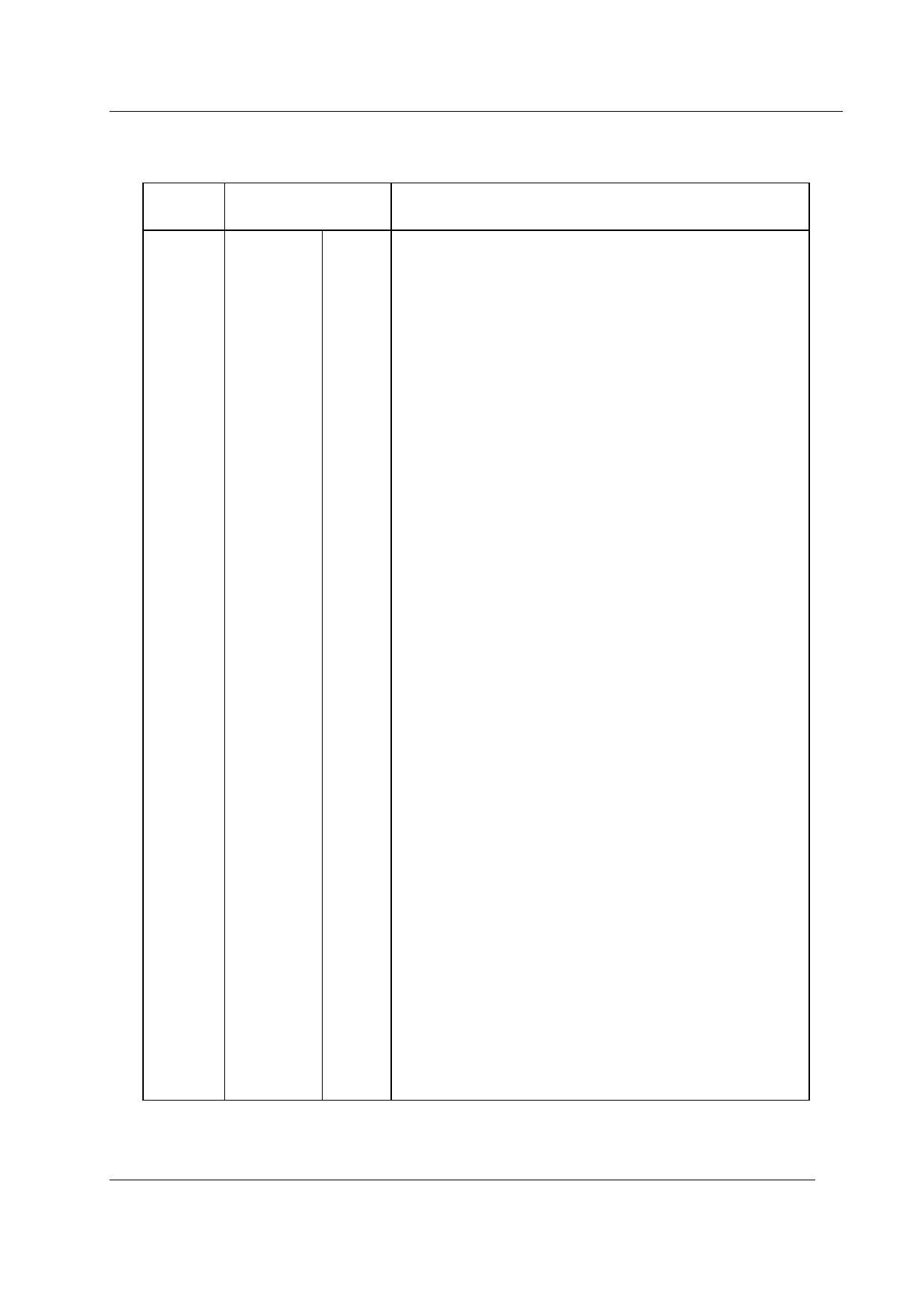
1.3 Signal List
CMX625
D5/P4
Pin No.
1
2
3
4
5
6
7
8
9
10
11
Signal
Name
FSC
Type
I/P
Description
The IOM-2 Frame Synchronisation Clock. This is an 8kHz
clock indicating the start of the frame. FSC is generated
by the upstream device. See section 1.5.1, 1.5.2 and
1.5.3.
DCL
I/P The IOM-2 Data Clock. It is used to clock data on and off
the bus and operates at 1.536MHz for Terminal mode
(TE) or 4.096MHz for non-Terminal mode (non-TE or Line
Card mode). DCL is generated by the upstream device.
When the bus is deactivated, DCL is held in a low state.
See section 1.5.1, 1.5.2 and 1.5.3.
DD
BI The IOM-2 Data Downstream, receives data from the
network. When the bus is deactivated or when data is not
being transmitted, DD is high impedance. The IC Channel
Bus Reversal (TE mode only) allows IC1 and IC2 data to
be transmitted on the DD pin. See section 1.5.1, 1.5.2,
1.5.3 and 1.5.6. An external pull-up resistor is required.
DU
BI The IOM-2 Data Upstream, transmits data to the network.
When the bus is deactivated or when data is not being
transmitted, DU is high impedance. The IC Channel Bus
Reversal (TE mode only) allows IC1 and IC2 data to be
received on the DU pin. See section 1.5.1, 1.5.2, 1.5.3
and 1.5.6. An external pull-up resistor is required.
TE/NTE
I/P The IOM-2 two modes of operation: TE = 0 selects
Terminal mode. NTE = 1 selects Non-Terminal mode or
Line Card mode. See section 1.5.1, 1.5.2 and 1.5.3.
SA0
I/P ) The IOM-2 Slot Address, provides one of 8 unique
SA1
I/P ) addresses. It allows the device to be individually
SA2
I/P ) addressed when more than one device is connected
) to the IOM-2 bus. See section 1.5.2 and 1.5.3.
DS
I/P The IOM-2 Device Select pin (NTE mode only). Allows two
CMX625 devices sharing a Slot Address to be individually
addressed. DS = 0 selects device one. DS = 1 selects
device two. See section 1.5.2 and 1.5.3.
RESET
I/P The external reset pin clears all the registers. (RESET=1)
IRQN
O/P A ‘wire-Orable’ output Interrupt Request. This output is
pulled down to VSS when active and is high impedance
when inactive. An external pull-up resistor is required.
2001 Consumer Microcircuits Limited
4
D/625/2
Share Link: 