CMPWR160SAR Ver la hoja de datos (PDF) - California Micro Devices Corp
Número de pieza
componentes Descripción
Fabricante
CMPWR160SAR Datasheet PDF : 10 Pages
| |||
CALIFORNIA MICRO DEVICES
CMPWR160
Typical Thermal Characteristics
Thermal dissipation of junction heat consists primarily of
two paths in series. The first path is the junction to the
case (θJC) thermal resistance which is defined by the
package style, and the second path is the case to
ambient (θCA) thermal resistance, which is dependent on
board layout.
The overall junction to ambient (θJA) thermal resistance is
equal to:
θJA = θJC + θCA
For a given package style and board layout, the operat-
ing junction temperature is a function of junction power
dissipation P , and the ambient temperature, resulting
JUNC
in the following thermal equation:
TJUNC = TAMB + PJUNC (θJC ) + PJUNC (θCA )
= TAMB + PJUNC (θJA)
The CMPWR160SA is housed in a thermally enhanced
package where all the GND pins (5 through 8) are
integral to the leadframe (fused leadframe). When the
device is mounted on a double sided printed circuit
board with two square inches of copper allocated for
“heat spreading”, the resulting θJA is 50°C/W.
Based on a maximum power dissipation of
1.0W (2Vx500mA) with an ambient of 70°C the resulting
junction temperature will be:
TJUNC = TAMB + PJUNC (θJA )
= 70°C + 1.0W (50°C/W)
= 70°C + 50°C = 120°C
All thermal characteristics of the CMPWR160SA were
measured using a double sided board with two square
inches of copper area connected to the GND pins for
“heat spreading”.
Measurements showing performance up to junction
temperature of 125°C were performed under light load
conditions (5mA). This allows the ambient temperature to
be representative of the internal junction temperature.
Note: The use of multi-layer board construction with
power planes will further enhance the thermal perfor-
mance of the package. In the event of no copper area
being dedicated for heat spreading, a multi-layer board
construction, using only the minimum size pad layout,
will typically provide the CMPWR160SA with an overall
θJA of 70°C/W which allows up to 780mW to be safely
dissipated.
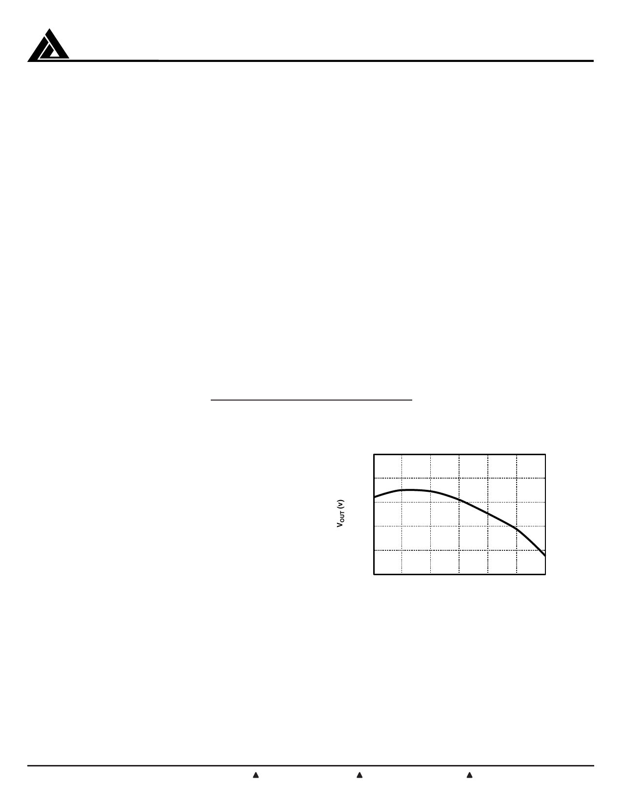
Output Voltage vs. Temperature
Figure 14 shows the regulator V performance up to
OUT
the maximum rated junction temperature. A 125°C
variation in junction temperature from –25°C causes an
output voltage variation of about 50mV, reflecting
a voltage temperature coefficient of approximately
±50ppm/°C.
3.35
3.33
3.31
3.29
3.27
3.25
–25
0
25
50
75
Temperature (˚C)
100 125
Figure 14. VOUT Temperature Variation (5mA)
©2000 California Micro Devices Corp. All rights reserved. SmartOR™ is a trademark of California Micro Devices Corporation.
215 Topaz Street, Milpitas, California 95035 Tel: (408) 263-3214
Fax: (408) 263-7846
www.calmicro.com
12/5/2000
9
Share Link: 