CMPWR150A/R Ver la hoja de datos (PDF) - California Micro Devices Corp
NГәmero de pieza
componentes DescripciГіn
Fabricante
CMPWR150A/R Datasheet PDF : 8 Pages
| |||
CALIFORNIA MICRO DEVICES
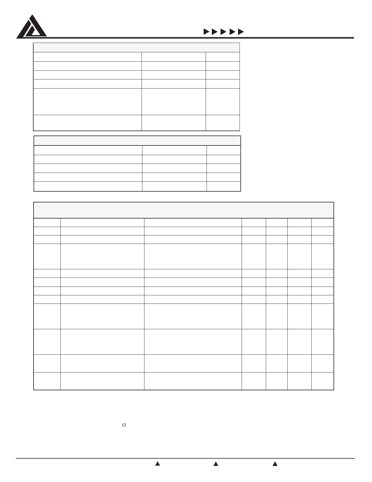
ABSOLUTE MAXIMUM RATINGS
Parameter
Rating
ESD Protection (HBM)
2000
VCC Input Voltage
Drive Logic Voltage
Storage Temperature Range
+6.0, Gnd -0.5
VCC +0.5, Gnd -0.5
-40 to +150
Operating Ambient
0 to +70
Operating Junction
0 to +125
Power Dissipation: TO-263
SOIC Note1
1.0
OPERATING CONDITIONS
Parameter
Range
VCC
Temperature (Ambient)
5.0 Вұ 0.5
0 to +70
Load Current
0 to 500
C EXT
10 Вұ 10%
Unit
V
V
V
oC
W
Unit
V
oC
mA
mF
CMPWR150
ELECTRICAL OPERATING CHARACTERISTICS
(over operating conditions unless specified otherwise)
Symbol Parameter
Conditions
MIN TYP MAX UNIT
VOUT
IO U T
VCCSEL
VCCD ES
VCCH Y ST
IS/C
IR CC
VR LOAD
VR LINE
ICC
IG N D
ROH
ROL
tD H
tD L
Regulator Output Voltage
Regulator Output Current
Select Voltage
Deselect Voltage
Hysteresis Voltage
Short Circuit Output Current
VCC Pin Reverse Leakage
Load Regulation
Line Regulation
Quiescent Supply current
Ground Pin Current Note 3
Drive Pull-up Resistance
Drive Pull-down Resistance
Drive High Delay
Drive Low Delay
500mA>ILOAD >0mA
Regulator Enabled
Regulator Disabled
Hysteresis Note 2
VCC = 5V, VOUT = 0V
VOUT = 3.3V, VCC = 0V
VCC = 5V, ILOAD = 50mA to 500mA
VCC = 4.5V to 5.5V, ILOAD = 5mA
VCC > VCCSEL, ILOAD = 0mA
VCCDES > VCC > VOUT
VOUT > VCC
Regulator Disabled
VCC = 5V, ILOAD = 5mA
VCC = 5V, ILOAD = 500mA
RPULLUP to VCC , VCC > VCCSEL
RPULLDOW N to GND, VCCDES > VCC
CDRIVE=1nF, VCC tRISE < 100ns
CDRIVE=1nF, VCC tFALL < 100ns
3.135 3.30 3.465 V
500 800
mA
4.35 4.45
3.90 4.10
V
0.25
1200
mA
5
50
mA
75
mV
2
mV
1.0
3.0
0.15 0.25 mA
0.01 0.02
0.15 0.30
1.0
2.5
mA
1.2 3.0
100 400
W
200 400
1.0
ms
0.2
Note 1:
Note 2:
Note 3:
The SOIC package used is thermally enhanced through the use of a fused integral leadframe. The power rating is based on a printed
circuit board heat spreading capability equivalent to 2 square inches of copper connected to the GND pins. Typical multi-layer boards
using power plane construction will provide this heat spreading ability without the need for additional dedicated copper area. (Please
consult with factory for thermal evaluation assistance.)
The hysteresis defines the maximum level of acceptable disturbance on VCC during switching. It is recommended that the VCC source
impedance be kept below 0.25в„Ұ to ensure the switching disturbance remains below the hysteresis during select/deselect transitions.
An input capacitor may be required to help minimize the switching transient.
Ground pin current consists of controller current (0.15mA) and regulator current if enabled. The controller always draws 0.15mA from
either VCC or VOUT , whichever is greater. All regulator current is supplied exclusively from VCC . At high load currents a small increase
occurs due to current limit protection circuitry.
В©1999 California Micro Devices Corp. All rights reserved.
2
215 Topaz Street, Milpitas, California 95035 Tel: (408) 263-3214 Fax: (408) 263-7846 www.calmicro.com
9/99
Share Link: 