TC1173 Ver la hoja de datos (PDF) - TelCom Semiconductor Inc => Microchip
Número de pieza
componentes Descripción
Fabricante
TC1173 Datasheet PDF : 7 Pages
| |||
300mA CMOS LDO With Shutdown,
ERROR Output, And Bypass
DETAILED DESCRIPTION
The TC1173 is a fixed output, low drop-out regulator.
Unlike bipolar regulators, the TC1173 supply current does not
increase with load current. In addition, VOUT remains stable and
within regulation at very low load currents (an important consid-
eration in RTC and CMOS RAM battery back-up applications).
TC1173 pin functions are detailed below:
PIN DESCRIPTIONS
Pin
No. Symbol Description
1
VOUT Regulated voltage output
2
GND Ground terminal
3
NC
No connect
4
Bypass Reference bypass input. Connecting a 470pF
to this input further reduces output noise.
5
ERROR Out-of-Regulation Flag (Open Drain Out-
put). This output goes low when VOUT is out-
of-tolerance by approximately -5%.
6
SHDN Shutdown control input. The regulator is fully
enabled when a logic high is applied to this
input. The regulator enters shutdown when a
logic low is applied to this input. During
shutdown, output voltage falls to zero and
supply current is reduced to 0.05µA (typical).
7
NC
No connect
8
VIN
Unregulated supply input
TC1173
SHDN may be controlled by a CMOS logic gate, or I/O port
of a microcontroller. If the SHDN input is not required, it
should be connected directly to the input supply. While in
shutdown, supply current decreases to 0.05µA (typical),
VOUT falls to zero and ERROR is disabled.
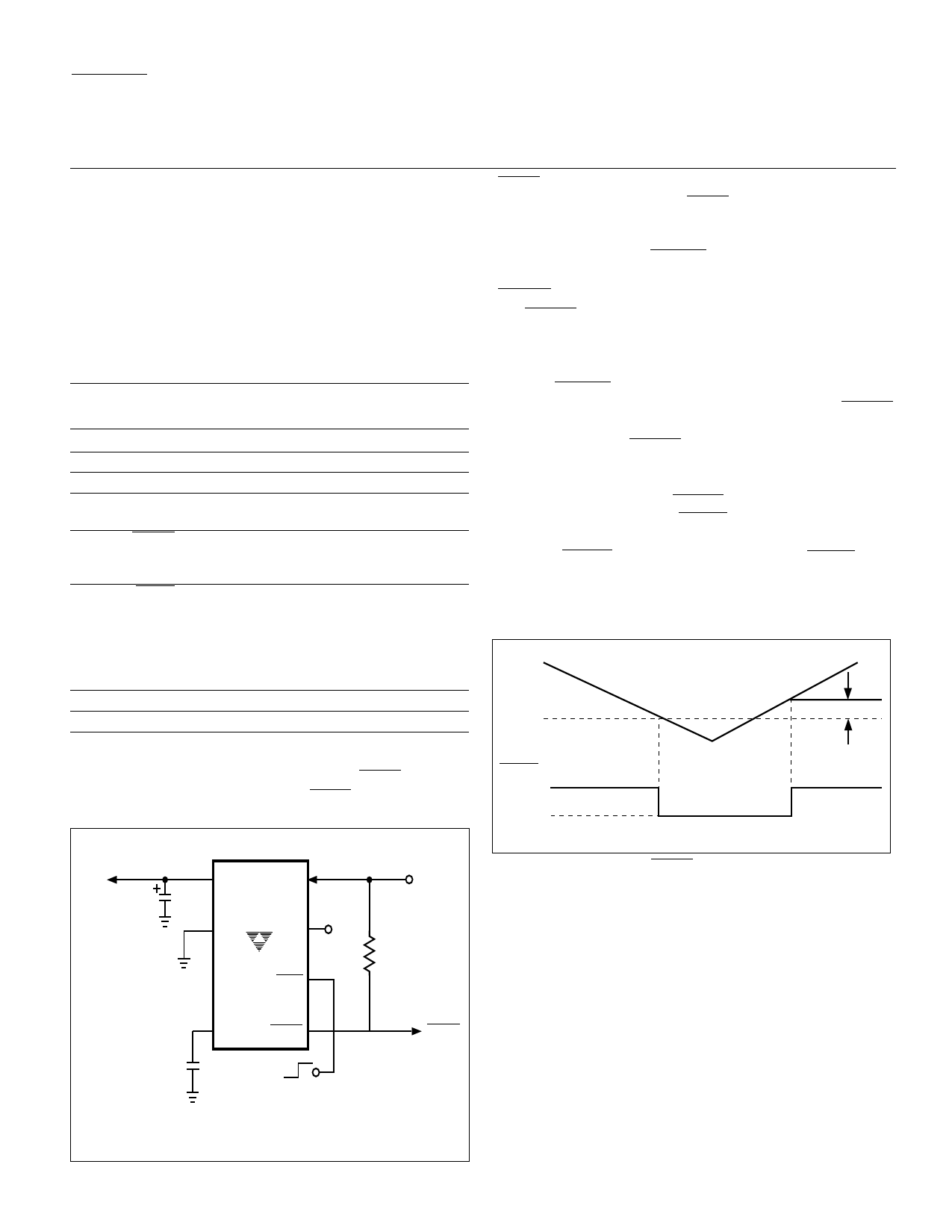
ERROR Output
ERROR is driven low whenever VOUT falls out of regu-
lation by more than – 5% (typical). This condition may be
caused by low input voltage, output current limiting, or
thermal limiting.
The ERROR threshold is 5% below rated VOUT regard-
less of the programmed output voltage value (e.g., ERROR
= VOL at 4.75V (typ) for a 5.0V regulator and 2.85V (typ) for
a 3.0V regulator). ERROR output operation is shown in
Figure 2. Note that ERROR is active when VOUT is at or
below VTH, and inactive when VOUT is above VTH + VH.
As shown in Figure 1, ERROR can be used as a battery
low flag, or as a processor RESET signal (with the addition
of timing capacitor C2). R1 x C3 should be chosen to
maintain ERROR below VIH of the processor RESET input
for at least 200msec to allow time for the system to stabilize.
Pull-up resistor R1 can be tied to VOUT, VIN or any other
voltage less than (VIN + 0.3V.)
VOUT
VTH
Hysteresis (VH)
Figure 1 shows a typical application circuit. The regula-
tor is enabled any time the shutdown input (SHDN) is above
VIH, and shutdown (disabled) when SHDN is at or below VIL.
ERROR
VIH
VOL
VOUT
TC1173-2 2/2/00
1
VOUT
C1
1µF
2
GND
8
VIN
7
NC
TC1173
3
6
NC
SHDN
VIN
R3
1M
4 Bypass
5
ERROR
ERROR
CBYPASS
470pF
(Optional)
Shutdown Control
(from Power Control Logic)
Figure 1: Typical Application Circuit
Figure 2: ERROR Output Operation
Output Capacitor
A 1µF (min) capacitor from VOUT to ground is recom-
mended. The output capacitor should have an effective
series resistance of 5Ω or less. A 1µF capacitor should be
connected from VIN to GND if there is more than 10 inches
of wire between the regulator and the AC filter capacitor, or
if a battery is used as the power source. Aluminum electro-
lytic or tantalum capacitor types can be used. (Since many
aluminum electrolytic capacitors freeze at approximately –
30°C, solid tantalums are recommended for applications
operating below – 25°C.) When operating from sources
other than batteries, supply-noise rejection and transient
response can be improved by increasing the value of the
input and output capacitors and employing passive filtering
techniques.
3
Share Link: 