TC1173 Ver la hoja de datos (PDF) - TelCom Semiconductor Inc => Microchip
Número de pieza
componentes Descripción
Fabricante
TC1173 Datasheet PDF : 7 Pages
| |||
300mA CMOS LDO With Shutdown,
ERROR Output, And Bypass
TC1173
ABSOLUTE MAXIMUM RATINGS*
Input Voltage .............................................................. 6.5V
Output Voltage ........................... (VSS – 0.3) to (VIN + 0.3)
Power Dissipation .................... Internally Limited (Note 7)
Operating Temperature .................... – 40°C < TJ < 125°C
Storage Temperature ............................ – 65°C to +150°C
Maximum Voltage on Any Pin ............ VIN +0.3V to – 0.3V
Lead Temperature (Soldering, 10 Sec.) ................ +300°C
*Absolute Maximum Ratings indicate device operation limits beyond dam-
age may occur. Device operation beyond the limits listed in Electrical
Characteristics is not recommended.
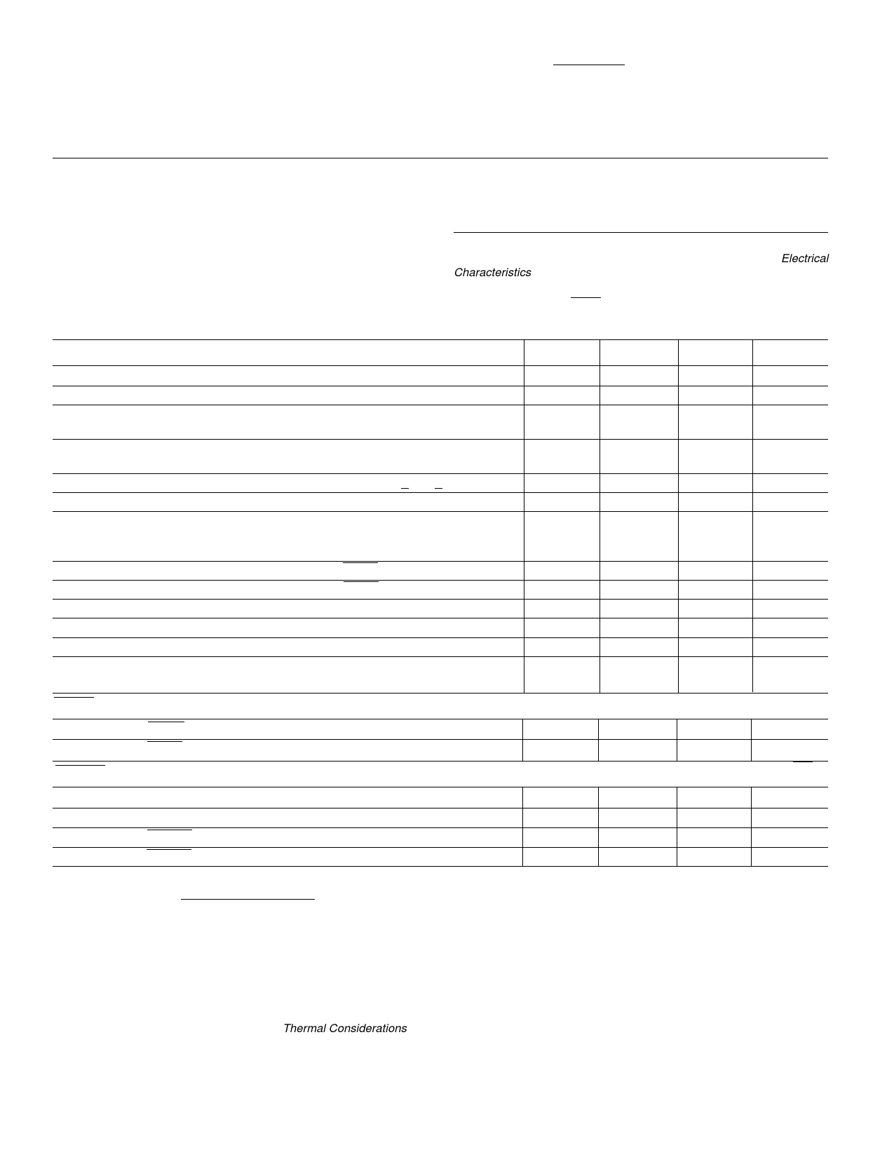
ELECTRICAL CHARACTERISTICS: VIN = VOUT + 1V, IL = 0.1µA, CL = 3.3µF, SHDN > VIH, TA = 25°C, unless otherwise noted.
BOLDFACE type specifications apply for junction temperatures of – 40°C to +125°C
Symbol
Parameter
Test Conditions
Min
Typ
Max
Units
VIN
IOUTMAX
VOUT
∆VOUT/∆T
∆VOUT/∆VIN
∆VOUT/VOUT
VIN – VOUT
ISS1
ISS2
PSRR
IOUTSC
∆VOUT∆PD
eN
Input Operating Voltage
Maximum Output Current
Output Voltage
VOUT Temperature Coefficient
Line Regulation
Load Regulation
Dropout Voltage (Note 4)
Supply Current
Shutdown Supply Current
Power Supply Rejection Ratio
Output Short Circuit Current
Thermal Regulation
Output Noise
Note 1
Note 2
—
300
—
VR - 2.5%
—
(VR + 1V) < VIN < 6V
—
IL = 0.1mA to IOUTMAX (Note 3)
—
IL = 0.1mA
—
IL = 100mA
IL = 300mA
SHDN = VIH
—
SHDN = 0V
—
FRE ≤ 1kHz
—
VOUT = 0V
—
Note 5
—
F = 1kHz, COUT = 1µF,
—
RLOAD = 50Ω
—
6.0
—
—
VR ± 0.5%
—
VR + 2.5%
—
—
40
0.05
0.35
0.5
2.0
20
30
80
160
240
480
50
90
0.05
0.5
60
—
550
650
0.04
—
260
—
V
mA
V
ppm/°C
%
%
mV
µA
µA
dB
mA
V/W
nV/√Hz
SHDN Input
VIH
SHDN Input High Threshold
VIL
SHDN Input Low Threshold
45
—
—
%VIN
—
—
15
%VIN
ERROR Output
VMIN
Minimum Operating Voltage
1.0
—
—
V
VOL
Output Logic Low Voltage
1mA Flows to ERROR
—
—
400
mV
VTH
ERROR Threshold Voltage
—
0.95 x VR
—
V
VOL
ERROR Positive Hysteresis Note 7
—
50
—
mV
NOTES: 1. VR is the user-programmed regulator output voltage setting.
2. TC VOUT = (VOUTMAX – VOUTMIN) x 10 6
VOUT x ∆T
3. Regulation is measured at a constant junction temperature using low duty cycle pulse testing. Load regulation is tested over a load range from 0.1mA
to the maximum specified output current. Changes in output voltage due to heating effects are covered by the thermal regulation specification.
4. Dropout voltage is defined as the input to output differential at which the output voltage drops 2% below its nominal value measured at a 1V differential.
5. Thermal Regulation is defined as the change in output voltage at a time T after a change in power dissipation is applied, excluding load
or line regulation effects. Specifications are for a current pulse equal to ILMAX at VIN = 6V for T = 10msec.
6. The maximum allowable power dissipation is a function of ambient temperature, the maximum allowable junction temperature, and the
thermal resistance from junction-to-air (i.e. TA, TJ, θJA). Exceeding the maximum allowable power dissipation causes the device to initiate
thermal shutdown. Please see Thermal Considerations section of this data sheet for more details.
7. Hysteresis voltage is referenced to VR.
TC1173-2 2/2/00
2
Share Link: 