CM3202-00SM Ver la hoja de datos (PDF) - California Micro Devices Corp
Número de pieza
componentes Descripción
Fabricante
CM3202-00SM Datasheet PDF : 12 Pages
| |||
PRELIMINARY
CM3202
Application Info (cont’d)
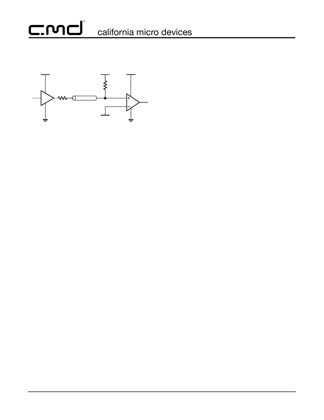
VDDQ
VTT (=VDDQ/2) VDDQ
Rs = 25
Line
Rt = 25
Transmitter
VREF (=VDDQ/2)
Receiver
Figure 1. Typical DDR terminations, Class II
The VTT power requirement is proportional to the num-
ber of data lines and the resistance of the termination
resistor, but does not vary with memory size. In a typi-
cal DDR data bus system each data line termination
may momentarily consume 16.2-mA to achieve the
405-mV minimum over VTT needed at the receiver:
Iterminaton = -R-4---t0--(-5-2---m5----Ω-V----) = 16.2mA
A typical 64 Mbyte SSTL-2 memory system, with 128
terminated lines, has a worst-case maximum VTT sup-
ply current up to ± 2.07A. However, a DDR memory
system is dynamic, and the theoretical peak currents
only occur for short durations, if they ever occur at all.
These high current peaks can be handled by the VTT
external capacitor. In a real memory system, the con-
tinuous average VTT current level in normal operation
is less than ± 200 mA.
The VDDQ power supply, in addition to supplying cur-
rent to the memory banks, could also supply current to
controllers and other circuitry. The current level typi-
cally stays within a range of 0.5A to 1A, with peaks up
to 2A or more, depending on memory size and the
computing operations being performed.
The tight tracking requirements and the need for VTT to
sink, as well as source, current provide unique chal-
lenges for powering DDR SDRAM.
CM3202 Regulator
The CM3202 dual output linear regulator provides all of
the power requirements of DDR memory by combining
two linear regulators into a single TDFN-8 or SOIC-8
package. VDDQ regulator can supply up to 2A current,
and the two-quadrant VTT termination regulator has
current sink and source capability to ±2A. The VDDQ
linear regulator uses a PMOS pass element for a very
low dropout voltage, typically 500mV at a 2A output.
The output voltage of VDDQ can be set by an external
voltage divider. The second output, VTT, is regulated at
VDDQ/2 by an internal resistor divider. The VTT regula-
tor can source, as well as sink, up to 2A current. The
CM3202 is designed for optimal operation from a nom-
inal 3.3VDC bus, but can work with VIN as high as 5V.
When operating at higher VIN voltages, attention must
be given to the increased package power dissipation
and proportionally increased heat generation.
VREF is typically routed to inputs with high impedance,
such as a comparator, with little current draw. An ade-
quate VREF can be created with a simple voltage
divider of precision, matched resistors from VDDQ to
ground. A small ceramic bypass capacitor can also be
added for improved noise performance.
Input and Output Capacitors
The CM3202 requires that at least a 220μF electrolytic
capacitor be located near the VIN pin for stability and to
maintain the input bus voltage during load transients.
An additional 4.7μF ceramic capacitor between the VIN
and the GND, located as close as possible to those
pins, is recommended to ensure stability.
A minimum of a 220μF electrolytic capacitor is recom-
mended for the VDDQ output. An additional 4.7μF
ceramic capacitor between the VDDQ and GND, located
very close to those pins, is recommended.
A minimum of a 220μF, electrolytic capacitor is recom-
mended for the VTT output. This capacitor should have
low ESR to achieve best output transient response. SP
or OSCON capacitors provide low ESR at high fre-
quency, and thus are a good choice. In addition, place
a 4.7μF ceramic capacitor between the VTT pin and
GND, located very close to those pins. The total ESR
must be low enough to keep the transient within the
VTT window of 40mV during the transition for source to
sink. An average current step of ± 0.5A requires:
ESR < 4----0---m-----V--- = 40mΩ
1A
Both outputs will remain stable and in regulation even
during light or no load conditions.
© 2006 California Micro Devices Corp. All rights reserved.
8 490 N. McCarthy Blvd., Milpitas, CA 95035-5112 l Tel: 408.263.3214 l Fax: 408.263.7846 l www.cmd.com
05/08/06
Share Link: 