CM3400 Ver la hoja de datos (PDF) - California Micro Devices Corp
Número de pieza
componentes Descripción
Fabricante
CM3400 Datasheet PDF : 9 Pages
| |||
CM3400
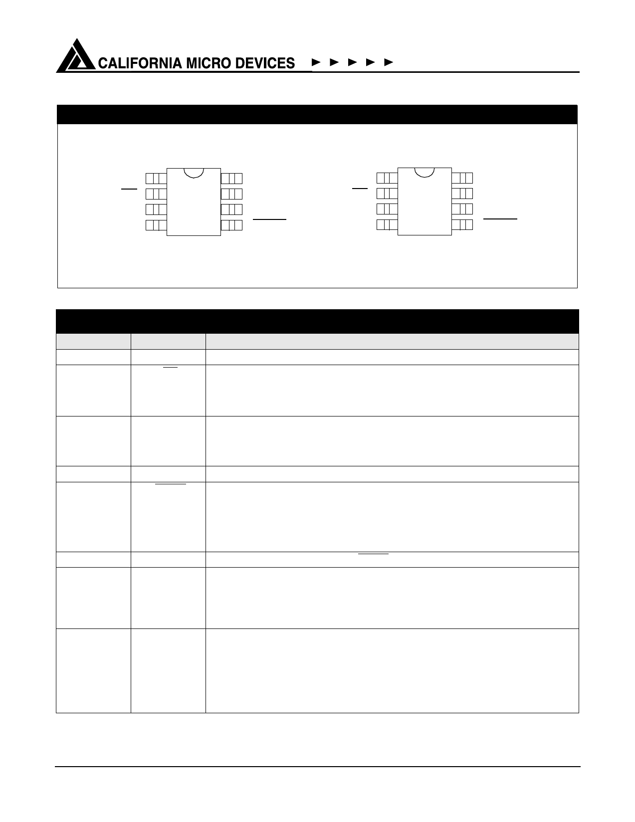
PACKAGE / PINOUT DIAGRAM
Top View
N.C.
MR
CT
GND
1
8
2
7
3
6
4
5
8-pin SOIC
Note: This drawing is not to scale.
VDD
SENSE
RESET
RESET
N.C.
MR
CT
GND
Top View
1
8
2
7
3
6
4
5
8-pin MSOP
VDD
SENSE
RESET
RESET
PIN(S)
1
2
3
4
5
6
7
8
NAME
N.C.
MR
CT
GND
RESET
RESET
SENSE
VDD
PIN DESCRIPTIONS
DESCRIPTION
No connect.
Active-Low manual reset control input. Whenever this input is taken logic low (grounded),
the device will immediately force a reset condition. Upon releasing from ground the reset
will remain active for the duration of the reset delay timing TDELAY interval. This contains
an internal pull-up current source and may be left unconnected if not used.
Capacitor timing control input. The timeout delay interval produced by the external timing
capacitor is 25ms/nF. A temperature stable internal current source (0.2µA) is used to
accurately control the user programmable delay interval. If no external timing capacitor is
present, the delay timeout interval is 25ms.
Negative reference for all voltages.
Active-low reset output. Whenever VOUT falls below the Reset threshold, the logic output
immediately is driven low (to GND). Upon VOUT rising above the Reset threshold, the
logic output remains low (at GND) for an additional delay time duration Td, after which it
is driven to a logic high level (set by VOUT). The power-on reset circuitry remains enabled
under all conditions and produces a valid output logic, even when VCC is not present.
Active-high reset output. Inverse of RESET.
Positive input voltage to the accurate 1.0 volt threshold comparator. Whenever this input
is below the trigger threshold (1.0V) both logic outputs are immediately held in their
respective Active state. When this input signal rises past the trigger threshold voltage,
the delay timer will start and both logic outputs will still remain Active. Once the delay
time has been reached both logic outputs will toggle to their respective Inactive state.
Input power source for the device. The device is designed to operate with supply voltage
of 2.5V or greater. Whenever the supply voltage is below 2.5V (i.e during power-up /
power-down) an internal undervoltage lockout circuit is activated which prevents any
false triggering on the RESET logic outputs. This feature ensures the logic outputs will
"hug" their respective rail and produce valid outputs under all supply conditions. (Con-
ventional Supervisory circuits can generate undefined output conditions during initial
power-up sequences)
© 2003 California Micro Devices Corp. All rights reserved.
2 430 N. McCarthy Blvd., Milpitas, CA 95035-5112 L Tel: 408.263.3214
L Fax: 408.263.7846 L www.calmicro.com
10/06/03
Share Link: 