CM313202SB Ver la hoja de datos (PDF) - California Micro Devices Corp
Número de pieza
componentes Descripción
Fabricante
CM313202SB Datasheet PDF : 11 Pages
| |||
PRELIMINARY
CM3132
Performance Information (cont’d)
Typical Thermal Characteristics
The overall junction to ambient thermal resistance
(θJA) for device power dissipation (PD) consists prima-
rily of two paths in series. The first path is the junction
to the case (θJC) which is defined by the package style,
and the second path is case to ambient (θCA) thermal
resistance which is dependent on board layout. The
final operating junction temperature for any set of con-
ditions can be estimated by the following thermal equa-
tion:
TJUNC = TAMB + PD ( θJC ) + PD ( θCA )
= TAMB + PD ( θJA)
When a CM3132-02SB (PSOP-8) is mounted on a
double-sided printed circuit board with two square
inches of copper allocated for "heat spreading," the
resulting θJA is 40°C/W. Based on the over tempera-
ture limit of 150° C with an ambient of 70°C, the avail-
able power of this package will be:
PD = -1---5---0-4---°0----C°----C-–---/--7--W-0----°----C-- = 2W
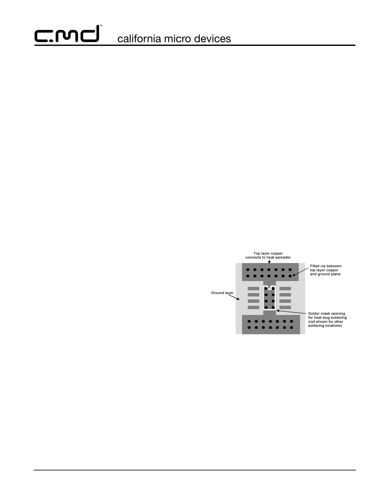
PCB Layout Considerations
The CM3132-02SB/SH has a heat spreader attached
to the bottom of the PSOP-8 package in order for heat
to be transferred more easily from the package to the
PCB. The heat spreader is a copper pad of dimensions
just smaller than the package itself. By positioning the
matching pad on the PCB top layer to connect to the
spreader during manufacturing, the heat will be trans-
ferred between the two pads. The drawing below
shows the recommended PCB layout. Note that there
are six vias on either side to allow the heat to dissipate
into the ground and power planes on the inner layers of
the PCB. Vias can be placed underneath the chip, but
this can cause blockage of the solder. The ground and
power planes should be at least 2 sq in. of copper by
the vias. It also helps dissipation if the chip is posi-
tioned away from the edge of the PCB, and not near
other heat-dissipating devices. A good thermal link
from the PCB pad to the rest of the PCB will assure the
best heat transfer from the CM3132 package to ambi-
ent, θJA, of around 40°C/W.
Figure 4. Recommended Heat Sink PCB Layout
© 2004 California Micro Devices Corp. All rights reserved.
8 430 N. McCarthy Blvd., Milpitas, CA 95035-5112 ● Tel: 408.263.3214 ● Fax: 408.263.7846 ● www.calmicro.com 10/13/04
Share Link: 