201002MR Ver la hoja de datos (PDF) - California Micro Devices Corp
Número de pieza
componentes Descripción
Fabricante
201002MR Datasheet PDF : 4 Pages
| |||
PRELIMINARY
CM2010
Specifications
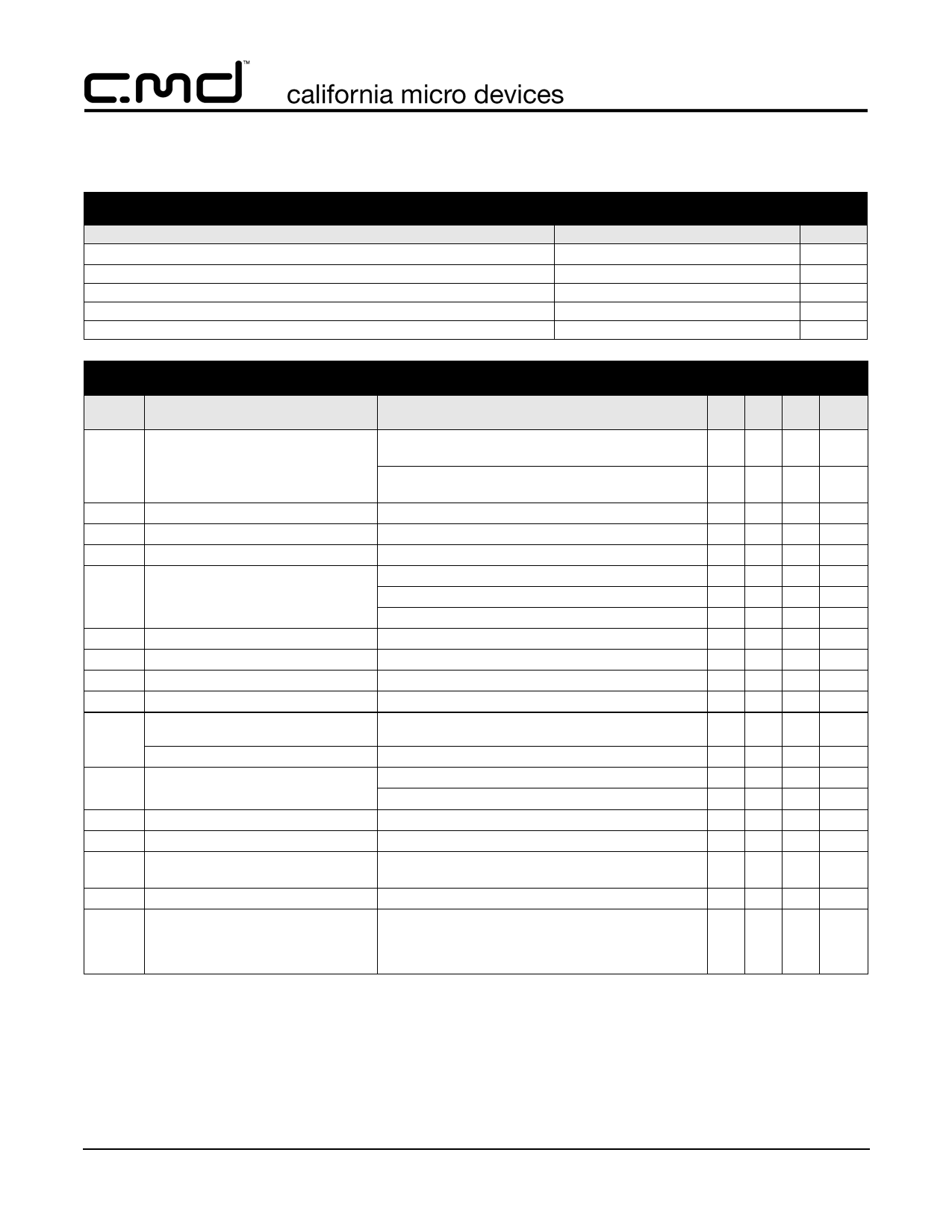
ABSOLUTE MAXIMUM RATINGS
PARAMETER
VCC_VIDEO and VCC_SYNC Supply Voltage Inputs
ESD Clamp Diode Forward DC Current (applies only to SYNC drivers)
DC Voltage at any channel Input
Operating Temperature Range
Storage Temperature Range
RATING
6.0
8
[GND - 0.5] to [VCC + 0.5]
-40 to +85
-40 to +150
UNITS
V
mA
V
°C
°C
ELECTRICAL OPERATING CHARACTERISTICS (SEE NOTE 1)
SYM-
BOL
PARAMETER
CONDITIONS
MIN TYP MAX UNITS
ICC VCC Supply Current
VCC_SYNC = 5V; SYNC inputs at GND or VCC_SYNC; SYNC
outputs unloaded
50 µA
VCC_SYNC = 5V; SYNC inputs at 3.0V;
SYNC outputs unloaded
2.0 mA
VF
VIH
VIL
VOH
VOL
ROUT
IIN
CIN_VID
tPLH
tPHL
tR, tF
Diode Forward Voltage
Logic High Input Voltage
Logic Low Input Voltage
Logic High Output Voltage
Logic Low Output Voltage
SYNC Driver Output Resistance
Input Current
VIDEO Inputs
SYNC_IN1, SYNC_IN2 Inputs
VIDEO Input Capacitance
SYNC Driver L => H Propagation Delay
SYNC Driver H => L Propagation Delay
SYNC Driver Output Rise & Fall Times
IF = 10mA
VCC_SYNC = 5.0V; Note 2
VCC_SYNC = 5.0V; Note 2
IOH = 8mA, VCC_SYNC = 3.0V; Note 2
IOH = 12mA, VCC_SYNC = 5.0V; Note 2
IOH = 24mA, VCC_SYNC = 5.0V; Note 2
IOL = 8mA, VCC_SYNC = 3.3V; Note 2
IOL = 12mA, VCC_SYNC = 5.0V; Note 2
IOL = 24mA, VCC_SYNC = 5.0V; Note 2
VCC_SYNC = 5.0V; SYNC Inputs at GND or 3.0V
VCC_VIDEO = 5.0V; VIN = VCC_VIDEO or GND; TA=25°C
VCC_SYNC = 5.0V; VIN = VCC_SYNC or GND; TA=25°C
VCC_VIDEO = 5.0V; VIN = 2.5V; ƒ = 1MHz; Note 4
VCC_VIDEO = 2.5V; VIN = 1.25V; ƒ = 1MHz; Note 4
CL = 10pF; VCC = 5.0V; Input tR and tF ≤ 5ns
CL = 10pF; VCC = 5.0V; Input tR and tF ≤ 5ns
CL = 10pF; VCC = 5.0V; Input tR and tF ≤ 5ns;
Notes 2, 4 & 5
1.0 V
1.5
V
0.5 V
2.0
V
2.0
V
2.0
V
0.8 V
0.8 V
0.8 V
15
Ω
±1 µA
±1 µA
4.0 pF
4.5 pF
12 ns
12 ns
3
ns
VESD
VCL
ESD Withstand Voltage
VCC_VIDEO = VCC_SYNC = 5V; Notes 3, 4
Clamping Voltage during ESD Discharge Notes 3 and 4
MIL-STD-883 (Method 3015), 8kV
Positive Transients
Negative Transients
±8
kV
+13
V
-13
V
Note 1: All parameters specified over standard operating conditions unless otherwise noted.
Note 2: These parameters apply only to the SYNC drivers.
Note 3: Per the IEC-61000-4-2 International ESD Standard, Level 4 contact discharge method. BYP, VCC must be bypassed to
GND via a low impedance ground plane with a 0.22µF, low inductance, chip ceramic capacitor at each supply pin. ESD
pulse is applied between the applicable pins and GND. ESD pulses can be positive or negative with respect to GND. Appli-
cable pins are: VIDEO_1, VIDEO_2 and VIDEO_3. All other pins are ESD protected to the industry standard ±2kV Human
Body Model (MIL-STD-883, Method 3015).
Note 4: This parameter is guaranteed by design and characterization.
Note 5: Rise and fall times measured between 0.5V and 2.4V.
© 2004 California Micro Devices Corp. All rights reserved.
09/10/04 430 N. McCarthy Blvd., Milpitas, CA 95035-5112 ● Tel: 408.263.3214 ● Fax: 408.263.7846 ● www.calmicro.com 3
Share Link: 