CM2006-02QR Ver la hoja de datos (PDF) - California Micro Devices Corp
Número de pieza
componentes Descripción
Fabricante
CM2006-02QR Datasheet PDF : 6 Pages
| |||
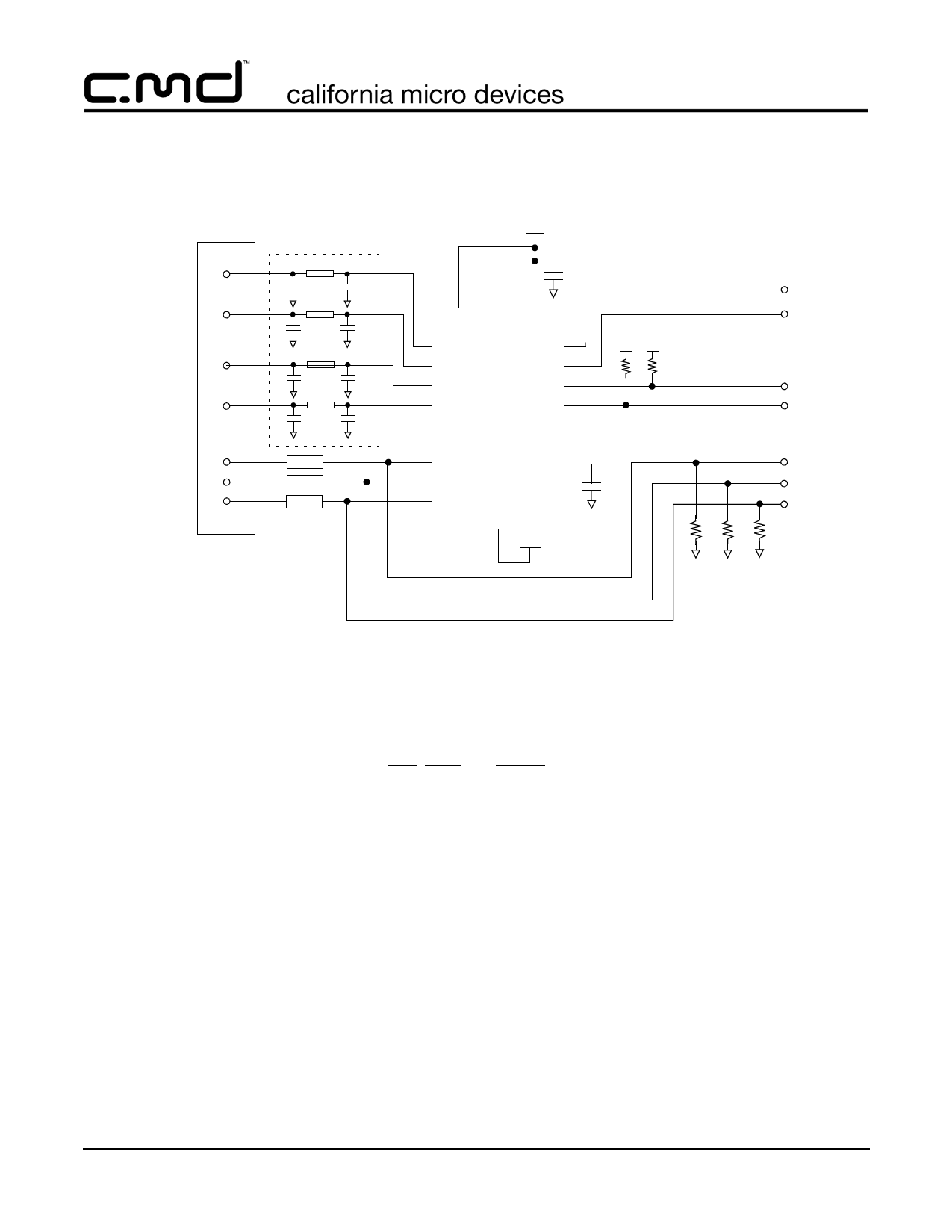
Application Information
VSYNC
HSYNC
DDCA_CLK
DDCA_DATA
Optional EMI Filters
C11
FB4
C12
C9
FB3
C10
C7
FB2
C8
C5
FB1
C6
RED_VIDEO
GREEN_VIDEO
BLUE_VIDEO
VF**
VF**
VF**
** VIDEO Filters.
Video Port
Connector
PRELIMINARY
CM2006
VCC_5V
0.22uF
ENABLE
VCC
SYNC_IN1 SYNC_OUT1
SYNC_IN2 SYNC_OUT2
DDC_IN1 DDC_OUT1
DDC_IN2 DDC_OUT2
CM2006
VIDEO_1
VIDEO_2
VIDEO_3
VCC_DDC
BYP
VCC_GPIO
RR
0.22uF
75 75 75
VSYNC
HSYNC
DDC_CLK
DDC_DATA
RED
GREEN
BLUE
Figure 1. Typical Application Connection Diagram
NOTES
1 The CM2006 should be placed as close to the VGA or DVI-I connector as possible.
2 The ESD protection channels VIDEO_1, VIDEO_2, VIDEO_3 may be used interchangeably between the R, G, B signals.
3 If differential video signal routing is used, the RED, BLUE, and GREEN signal lines should be terminated with external 37.5
ohm resistors.
4 "VF" are external video filters for the RGB signals.
5 Supply bypass capacitors C1 and C2 must be placed immediately adjacent to the corresponding Vcc pins. Connections to
the Vcc pins and ground plane must be made with minimal length copper traces (preferably less than 5mm) for best ESD
protection.
6 The bypass capacitor for the BYP pin has been omitted in this diagram. This results in a reduction in the maximum ESD
withstand voltage at the DDC_OUT pins from ±8kV to ±2kV. If 8kV ESD protection is required, a 0.22μF ceramic bypass
capacitor should be connected between BYP and ground.
7 The SYNC buffers may be used interchangeably between HSYNC and VSYNC.
8 The EMI filters at the SYNC_OUT and DDC_OUT pins (C5 to C12, and Ferrite Beads FB1 to FB4) are for reference only.
The component values and filter configuration may be changed to suit the application.
9 The DDC level shifters DDC_IN, DDC_OUT, may be used interchangeably between DDCA_CLK and DDCA_DATA.
10 R1, R2 are optional. They may be used, if required, to pull the DDC_CLK and DDC_DATA lines to VCC_5V when no mon-
itor is connected to the VGA connector. If used, it should be noted that "back current" may flow between the DDC pins and
VCC_5V via these resistors when VCC_5V is powered down.
© 2006 California Micro Devices Corp. All rights reserved.
02/21/06
490 N. McCarthy Blvd., Milpitas, CA 95035-5112 ● Tel: 408.263.3214 ● Fax: 408.263.7846 ● www.cmd.com 5
Share Link: 