CM1205 Ver la hoja de datos (PDF) - ON Semiconductor
Número de pieza
componentes Descripción
Fabricante
CM1205 Datasheet PDF : 5 Pages
| |||
CM1205
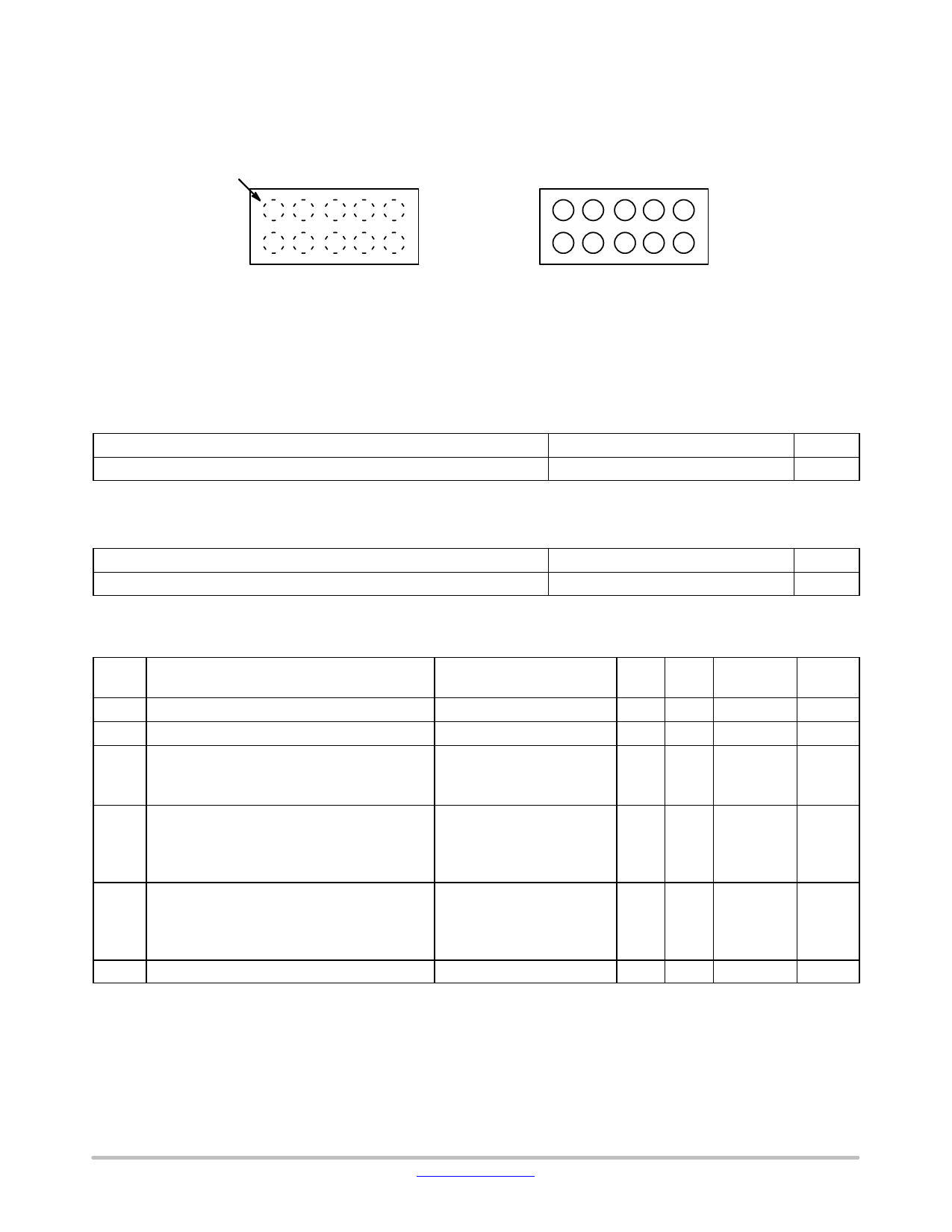
PACKAGE / PINOUT DIAGRAMS
Orientation
Marking
TOP VIEW
(Bumps Down View)
+
120508
BOTTOM VIEW
(Bumps Up View)
B1 B2 B3 B4 B5
A1 A2 A3 A4 A5
CM1205−08
10−bump CSP Package
SPECIFICATIONS
Table 1. ABSOLUTE MAXIMUM RATINGS
Parameter
Rating
Units
Storage Temperature Range
−65 to +150
°C
Stresses exceeding those listed in the Maximum Ratings table may damage the device. If any of these limits are exceeded, device functionality
should not be assumed, damage may occur and reliability may be affected.
Table 2. STANDARD OPERATING CONDITIONS
Parameter
Operating Temperature Range
Rating
−40 to +85
Units
°C
Table 3. ELECTRICAL OPERATING CHARACTERISTICS (Note 1)
Sym-
bol
Parameter
Conditions
Min Typ
Max
VREV
ILEAK
VSIG
Reverse Standoff Voltage
Leakage Current
Signal Clamp Voltage
Positive Clamp
Negative Clamp
IDIODE= 10 mA
VIN= 3.3 V DC
ILOAD= 10mA
6.0
100
5.6 6.8
8.0
−1.2 −0.8
−0.4
VESD In−system ESD Withstand Voltage
Note 2
a) Human Body Model, MIL−STD−883, Method
±30
3015
b) Contact Discharge per IEC 61000−4−2 Level 4
±25
VCL Clamping Voltage during ESD Discharge
MIL−STD−883 (Method 3015), 8 kV
Note 2
Positive Transients
+12
Negative Transients
−8
C Channel Capacitance
At 2.5 V DC, f = 1 MHz
39
47
1. TA = 25 °C unless otherwise specified. GND in this document refers to the lower supply voltage.
2. ESD applied to channel pins with respect to GND, one at a time. All other channels are open. All GND pins tied to ground.
Units
V
nA
V
kV
V
pF
www.onsemi.com
2
Share Link: 