CDP18243 Ver la hoja de datos (PDF) - Intersil
Número de pieza
componentes Descripción
Fabricante
CDP18243 Datasheet PDF : 5 Pages
| |||
CDP1824/3, CDP1824C/3
Absolute Maximum Ratings
DC Supply Voltage Range, (VDD)
(All Voltages Referenced to VSS Terminal)
CDP1824/3 . . . . . . . . . . . . . . . . . . . . . . . . . . . . . . . -0.5V to +11V
CDP1824C/3. . . . . . . . . . . . . . . . . . . . . . . . . . . . . . . . .-0.5 to +7V
Input Voltage Range, All Inputs . . . . . . . . . . . . . -0.5V to VDD +0.5V
DC Input Current, Any One Input . . . . . . . . . . . . . . . . . . . . . . . . ±10mA
Thermal Information
Thermal Resistance (Typical, Note 1)
θJA (oC/W) θJC (oC/W)
SBDIP Package. . . . . . . . . . . . . . . . . .
75
20
Device Dissipation Per Output Transistor
TA = Full Package Temperature Range
(All Package Types) . . . . . . . . . . . . . . . . . . . . . . . . . . . . . 100mW
Operating Temperature Range
Package Type D . . . . . . . . .
(TA)
....
.
.
.
.
.
.
.
.
.
.
.
. -55oC
to
+125oC
Storage Temperature Range (TSTG) . . . . . . . . . . .-65oC to +150oC
Lead Temperature (During Soldering)
At distance 1/16 ± 1/32 In. (1.59 ± 0.79mm)
from case for 10s max . . . . . . . . . . . . . . . . . . . . . . . . . . . . +265oC
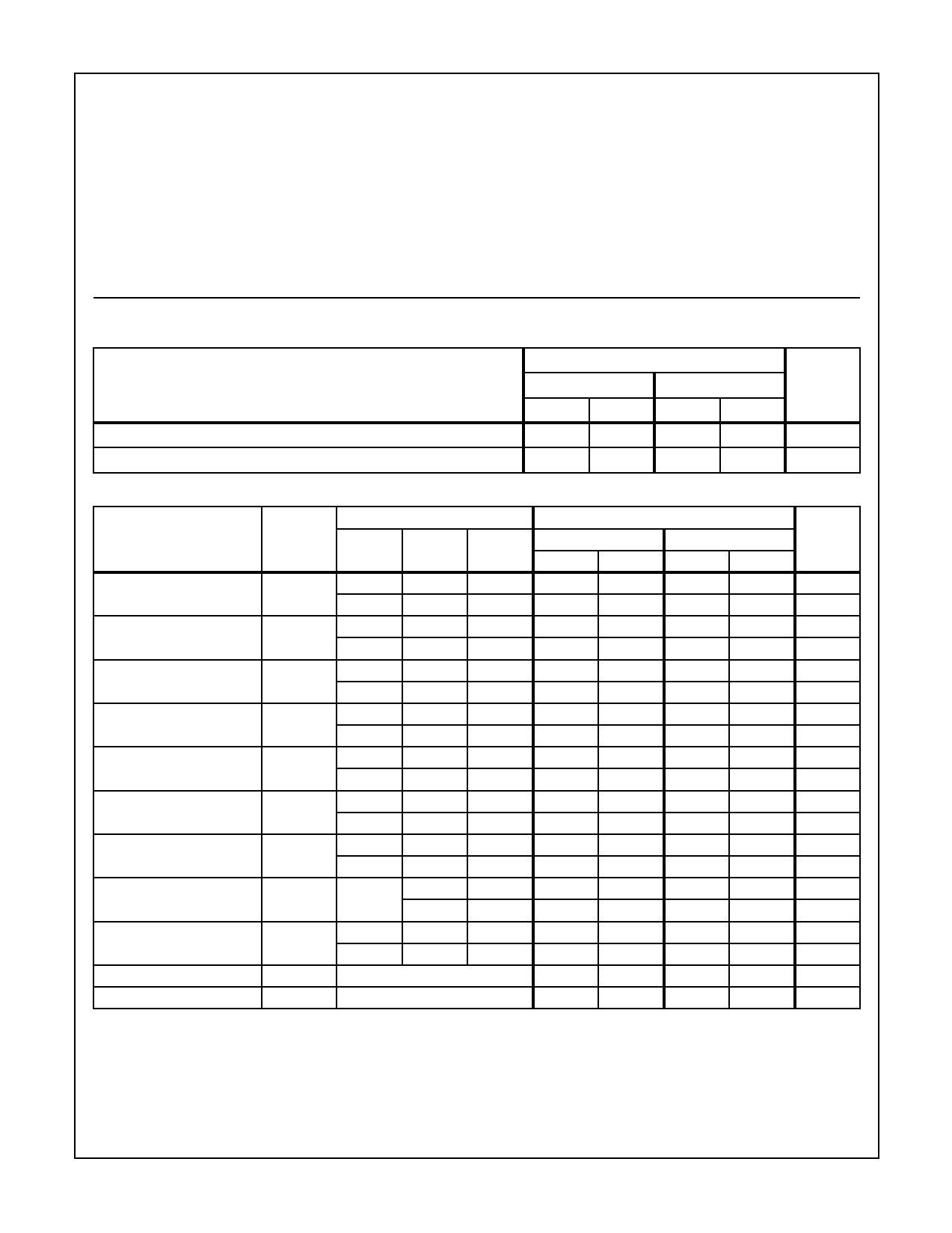
Recommended Operating Conditions TA = Full Package-Temperature Range. For maximum reliability, nominal operating
conditions should be selected so that operation is always within the following ranges:
PARAMETER
DC Operating Voltage Range
Input Voltage Range
LIMITS
CDP1824/3
CDP1824C/3
MIN
MAX
MIN
MAX
4
10.5
4
6.5
VSS
VDD
VSS
VDD
UNITS
V
V
Static Electrical Specifications
PARAMETER
SYMBOL
CONDITIONS
VO
VIN
VDD
(V)
(V)
(V)
LIMITS
-55oC, +25oC
+125oC
MIN
MAX
MIN
MAX
UNITS
Quiescent Device Current
IDD
(Note 1)
-
0, 5
5
-
0, 10
10
-
50
-
500
µA
-
500
-
1000
µA
Output Voltage Low-Level
VOL
-
0, 5
5
-
0.1
-
0.2
V
(Note 2)
-
10
-
0.1
-
0.2
V
Output Voltage High-Level
VOH
-
0, 5
5
4.9
-
4.8
-
V
(Note 2)
-
-
10
9.9
-
4.8
-
V
Input Low Voltage
VIL
0.5, 4.5
-
5
-
1.5
-
1.5
V
1, 9
-
10
-
3
-
-
V
Input High Voltage
VIH
0.5, 4.5
-
5
3.5
-
3.5
-
V
1, 9
-
10
7
-
7
-
V
Output Low Drive (Sink)
Current
IOL
0.4
0, 5
5
4
0.5
0, 10
10
4
-
1.5
-
mA
-
2.9
-
mA
Output High Drive (Source)
IOH
4.6
0, 5
5
-
-1
-
-0.75
mA
Current
9.5
0, 10
10
-
-2
-
-1.5
mA
Input Current
IIN
Any
0, 5
5
-
±1
-
±5
µA
Input
0, 10
10
-
±1
-
±5
µA
Three-State Output
Leakage Current
IOUT
0, 5
0, 5
5
-
±2
-
±5
µA
0, 10
0, 10
10
-
±2
-
±5
µA
Input Capacitance
Output Capacitance
NOTES:
CIN
COUT
(Note 2)
(Note 2)
-
10
-
10
pF
-
15
-
15
pF
1. The CDP1824C/3 meets all 5V Static Electrical Characteristics of the CDP1824/3 except Quiescent Device Current for which the limits
are IDD = 200µA at +25oC/-55oC; IDD = 1000µA at +125oC.
2. Guaranteed, but not tested.
43
Share Link: 