CDP1802AC/3 Ver la hoja de datos (PDF) - Intersil
Número de pieza
componentes Descripción
Fabricante
CDP1802AC/3 Datasheet PDF : 27 Pages
| |||
CDP1802AC/3
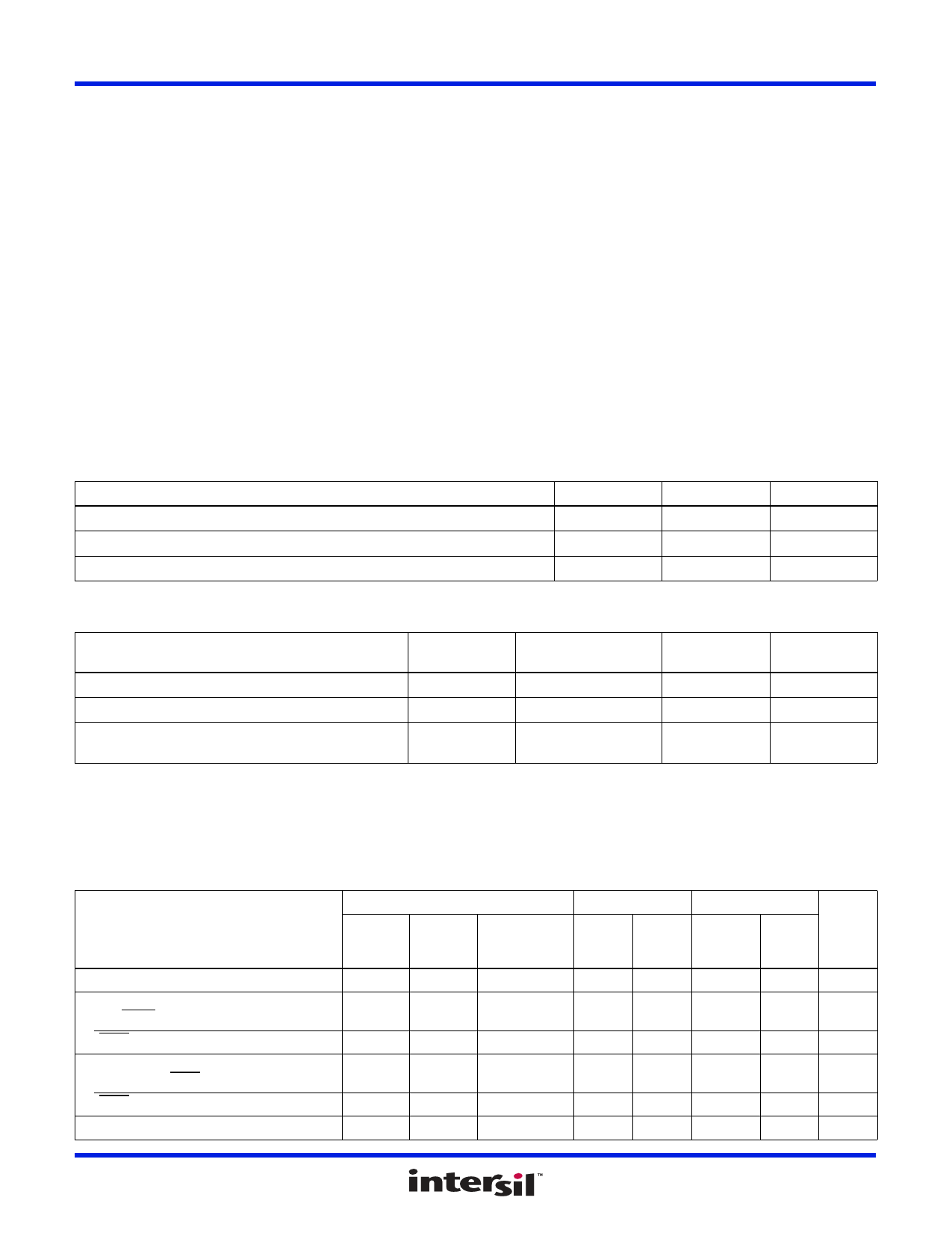
Absolute Maximum Ratings
DC Supply Voltage Range, (VDD)
(All Voltages Referenced to VSS Terminal)
CDP1802AC/3 . . . . . . . . . . . . . . . . . . . . . . . . . . . . . . . -0.5V to +7V
Input Voltage Range, All Inputs . . . . . . . . . . . . . -0.5V to VDD +0.5V
DC Input Current, any One Input . . . . . . . . . . . . . . . . . . . . . . ±10mA
Thermal Information
Thermal Resistance (Typical, Notes 1, 2) JA (°C/W) JC (°C/W)
SBDIP Package . . . . . . . . . . . . . . . . . .
55
15
Device Dissipation Per Output Transistor
TA = Full Package Temperature Range . . . . . . . . . . . . . . .100mW
Operating Temperature Range (TA)
Package Type D. . . . . . . . . . . . . . . . . . . . . . . . . .-55°C to +125°C
Storage Temperature Range (TSTG) . . . . . . . . . . . .-65°C to +150°C
Lead Temperature (During Soldering)
At distance 1/16 ± 1/32 In. (1.59 ±0.79mm)
from case for 10s max . . . . . . . . . . . . . . . . . . . . . . . . . . . . +265°C
Pb-Free Reflow Profile. . . . . . . . . . . . . . . . . . . . . . . . .see link below
http://www.intersil.com/pbfree/Pb-FreeReflow.asp
CAUTION: Do not operate at or near the maximum ratings listed for extended periods of time. Exposure to such conditions may adversely impact product reliability and
result in failures not covered by warranty.
NOTES:
1. JA is measured with the component mounted on a high effective thermal conductivity test board in free air. See Tech Brief TB379 for details.
2. For JC, the “case temp” location is the center of the exposed metal pad on the package underside.
Recommended Operating Conditions
TA = Full Package Temperature Range. For maximum reliability, operating conditions should
be selected so that operation is always within the following ranges. Parameters with MIN
and/or MAX limits are 100% tested at +25°C, unless otherwise specified. Temperature limits
established by characterization and are not production tested.
PARAMETER
MIN
MAX
UNITS
DC Operating Voltage Range
4
6.5
V
Input Voltage Range
Maximum Clock Input Rise or Fall Time
VSS
VDD
V
-
1
µs
Performance Specifications Parameters with MIN and/or MAX limits are 100% tested at +25°C, unless otherwise specified.
Temperature limits established by characterization and are not production tested.
PARAMETER
VDD
(V)
-55°C TO +25°C
+125°C
UNITS
Minimum Instruction Time (Note 3)
5
4.5
5.9
µs
Maximum DMA Transfer Rate
5
450
340
Kbytes/s
Maximum Clock Input Frequency,
Load Capacitance (CL) = 50pF, fCL
5
DC-3.6
DC-2.7
MHz
NOTE:
3. Equals 2 machine cycles - one Fetch and one Execute operation for all instructions except Long Branch and Long Skip, which require 3 machine
cycles - one Fetch and two Execute operations.
Static Electrical Specifications All Limits are 100% Tested. Parameters with MIN and/or MAX limits are 100% tested at +25°C,
unless otherwise specified. Temperature limits established by characterization and are not
production tested.
CONDITIONS
-55°C, +25°C
+125°C
PARAMETER
VOUT
VIN,
(V)
(V)
VCC, VDD
(V)
(Note 4)
MIN
MAX
MIN
MAX UNITS
Quiescent Device Current, IDD
Output Low Drive (Sink) Current
(Except XTAL), IOL
XTAL
-
-
0.4
0, 5
0.4
5
5
-
100
-
250
µA
5
1.20
-
0.90
-
mA
5
185
-
140
-
µA
Output High Drive (Source)
Current (Except XTAL), IOH
XTAL
4.6
0, 5
5
4.6
0
5
-
-0.30
-
-0.20
mA
-
-135
-
-100
µA
Output Voltage Low-Level, VOL
-
0, 5
5
-
0.1
-
0.2
V
FN1441 Rev 3.00
October 17, 2008
Page 4 of 27
Share Link: 