CAV24C64 Ver la hoja de datos (PDF) - ON Semiconductor
Número de pieza
componentes Descripción
Fabricante
CAV24C64 Datasheet PDF : 10 Pages
| |||
CAV24C64
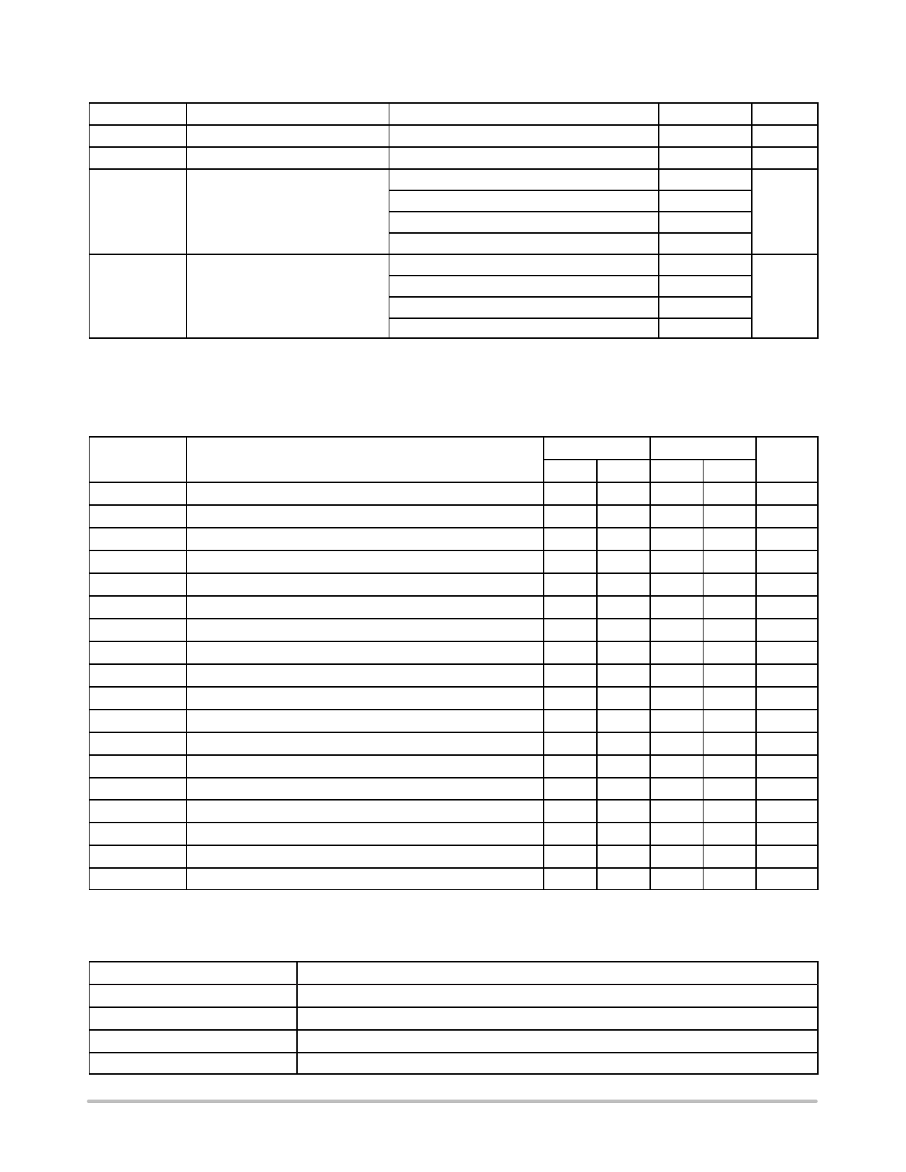
Table 4. PIN IMPEDANCE CHARACTERISTICS (VCC = 2.5 V to 5.5 V, TA = −40°C to +125°C, unless otherwise specified.)
Symbol
Parameter
Conditions
Max
Units
CIN (Note 4) SDA I/O Pin Capacitance
VIN = 0 V, TA = 25°C
8
pF
CIN (Note 4) Input Capacitance (other pins)
VIN = 0 V, TA = 25°C
6
pF
IWP (Note 5) WP Input Current
VIN < VIH, VCC = 5.5 V
130
mA
VIN < VIH, VCC = 3.3 V
120
VIN < VIH, VCC = 2.5 V
80
VIN > VIH
2
IA (Note 5)
Address Input Current
(A0, A1, A2)
Product Rev F
VIN < VIH, VCC = 5.5 V
VIN < VIH, VCC = 3.3 V
VIN < VIH, VCC = 2.5 V
50
mA
35
25
VIN > VIH
2
4. These parameters are tested initially and after a design or process change that affects the parameter according to appropriate AEC−Q100
and JEDEC test methods.
5. When not driven, the WP, A0, A1 and A2 pins are pulled down to GND internally. For improved noise immunity, the internal pull−down is relatively
strong; therefore the external driver must be able to supply the pull−down current when attempting to drive the input HIGH. To conserve power,
as the input level exceeds the trip point of the CMOS input buffer (~ 0.5 x VCC), the strong pull−down reverts to a weak current source.
Table 5. A.C. CHARACTERISTICS (VCC = 2.5 V to 5.5 V, TA = −40°C to +125°C, unless otherwise specified.) (Note 6)
Standard
Fast
Symbol
Parameter
Min
Max
Min
Max
Units
FSCL
Clock Frequency
100
400
kHz
tHD:STA
START Condition Hold Time
4
0.6
ms
tLOW
Low Period of SCL Clock
4.7
1.3
ms
tHIGH
High Period of SCL Clock
4
0.6
ms
tSU:STA
START Condition Setup Time
4.7
0.6
ms
tHD:DAT
Data In Hold Time
0
0
ms
tSU:DAT
Data In Setup Time
250
100
ns
tR
SDA and SCL Rise Time
1000
300
ns
tF (Note 6)
SDA and SCL Fall Time
300
300
ns
tSU:STO
STOP Condition Setup Time
4
0.6
ms
tBUF
Bus Free Time Between STOP and START
4.7
1.3
ms
tAA
SCL Low to Data Out Valid
3.5
0.9
ms
tDH
Data Out Hold Time
100
100
ns
Ti (Note 6)
Noise Pulse Filtered at SCL and SDA Inputs
100
100
ns
tSU:WP
WP Setup Time
0
0
ms
tHD:WP
WP Hold Time
2.5
2.5
ms
tWR
Write Cycle Time
5
5
ms
tPU (Notes 7, 8) Power−up to Ready Mode
1
1
ms
6. Test conditions according to “AC Test Conditions” table.
7. Tested initially and after a design or process change that affects this parameter.
8. tPU is the delay between the time VCC is stable and the device is ready to accept commands.
Table 6. A.C. TEST CONDITIONS
Input Levels
Input Rise and Fall Times
0.2 x VCC to 0.8 x VCC
≤ 50 ns
Input Reference Levels
Output Reference Levels
Output Load
0.3 x VCC, 0.7 x VCC
0.5 x VCC
Current Source: IOL = 3 mA; CL = 100 pF
http://onsemi.com
3
Share Link: 