CAT28LV65 Ver la hoja de datos (PDF) - ON Semiconductor
Número de pieza
componentes Descripción
Fabricante
CAT28LV65 Datasheet PDF : 15 Pages
| |||
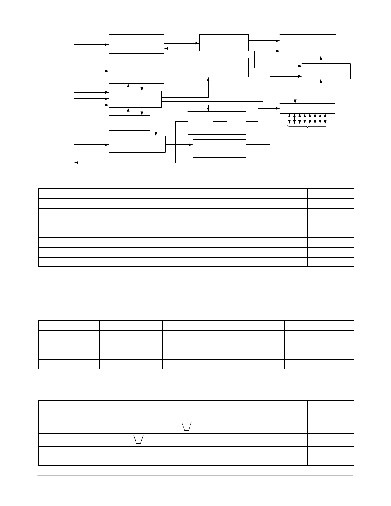
CAT28LV65
A5−A12
VCC
ADDR. BUFFER
& LATCHES
INADVERTENT
WRITE
PROTECTION
ROW
DECODER
HIGH VOLTAGE
GENERATOR
8,192 x 8
E2PROM
ARRAY
32 BYTE PAGE
REGISTER
CE
OE
WE
A0−A4
RDY/BUSY
CONTROL
LOGIC
TIMER
ADDR. BUFFER
& LATCHES
DATA POLLING
RDY/BUSY &
TOGGLE BIT
COLUMN
DECODER
Figure 1. Block Diagram
I/O BUFFERS
I/O0−I/O7
Table 1. ABSOLUTE MAXIMUM RATINGS
Parameters
Ratings
Units
Temperature Under Bias
–55 to +125
°C
Storage Temperature
–65 to +150
°C
Voltage on Any Pin with Respect to Ground (Note 1)
VCC with Respect to Ground
Package Power Dissipation Capability (TA = 25°C)
Lead Soldering Temperature (10 secs)
–2.0 V to +VCC + 2.0 V
V
−2.0 to +7.0
V
1.0
W
300
°C
Output Short Circuit Current (Note 2)
100
mA
Stresses exceeding Maximum Ratings may damage the device. Maximum Ratings are stress ratings only. Functional operation above the
Recommended Operating Conditions is not implied. Extended exposure to stresses above the Recommended Operating Conditions may affect
device reliability.
1. The minimum DC input voltage is −0.5 V. During transitions, inputs may undershoot to −2.0 V for periods of less than 20 ns. Maximum DC
voltage on output pins is VCC + 0.5 V, which may overshoot to VCC + 2.0 V for periods of less than 20 ns.
2. Output shorted for no more than one second. No more than one output shorted at a time.
Table 2. RELIABILITY CHARACTERISTICS (Note 3)
Symbol
Parameter
Test Method
Min
Max
NEND
Endurance
MIL−STD−883, Test Method 1033
105
TDR
Data Retention
MIL−STD−883, Test Method 1008
100
VZAP
ESD Susceptibility
MIL−STD−883, Test Method 3015
2,000
ILTH (Note 4)
Latch−Up
JEDEC Standard 17
100
3. These parameters are tested initially and after a design or process change that affects the parameters.
4. Latch−up protection is provided for stresses up to 100 mA on address and data pins from −1 V to VCC + 1 V.
Table 3. MODE SELECTION
Mode
CE
WE
OE
I/O
Read
L
H
L
DOUT
Byte Write (WE Controlled)
L
H
DIN
Byte Write (CE Controlled)
L
H
DIN
Standby and Write Inhibit
H
X
X
High−Z
Read and Write Inhibit
X
H
H
High−Z
Units
Cycles/Byte
Years
V
mA
Power
ACTIVE
ACTIVE
ACTIVE
STANDBY
ACTIVE
http://onsemi.com
3
Share Link: 