CA3280(2002) Ver la hoja de datos (PDF) - Intersil
Número de pieza
componentes Descripción
Fabricante
CA3280 Datasheet PDF : 10 Pages
| |||
CA3280, CA3280A
Application Information
Figures 4 and 5 show the equivalent circuits for the current
source and linearization diodes in the CA3280. The current
through the linearization network is approximately equal to the
programming current. There are several advantages to driving
these diodes with a current source. First, only the offset current
from the biasing network flows through the input resistor.
Second, another input is provided to extend the gain control
dynamic range. And third, the input is truly differential and can
accept signals within the common mode range of the CA3280.
Typical Applications
The structure of the variable operational amplifier eliminates
the need for matched resistor networks in differential to single
ended converters, as shown in Figure 6. A matched resistor
network requires ratio matching of 0.01% or trimming for 80dB
of common-mode rejection. The CA3280, with its excellent
common mode rejection ratio, is capable of converting a small
(±25mV) differential input signal to a single-ended output
without the need for a matched resistor network.
Figure 7 shows the CA3280 in a typical gain control application.
Gain control can be performed with the amplifier bias current
V+
RD = SMALL SIGNAL DIODE
IMPEDANCE
RD
≈ 52Ω
ID(mA)
x 1.34 =
70
ID
VOA
(lABC). With no diode bias current, the gain is merely gMRL. For
example, with an lABC of 1mA, the gM is approximately 16mS.
With the CA3280 operating into a 5kΩ resistor, the gain is 80.
The need for external buffers can be eliminated by the use of
low value load resistors, but the resulting increase in the
required amplifier bias current reduces the input impedance
of the CA3280. The linearization diode impedance also
decreases as the diode bias current increases, which further
loads the input. The diodes, in addition to acting as a
linearization network, also operate as an additional
attenuation system to accommodate input signals in the volt
range when they are applied through appropriate input
resistors.
Figure 10 shows a triangle wave to sine wave converter
using the CA3280. Two 100kΩ resistors are connected
between the differential amplifier emitters and V+ to reduce
the current flow through the differential amplifier. This allows
the amplifier to fully cut off during peak input signal
excursions. THD is appropriately 0.37% for this circuit.
RD
VOA
IABC
ID
V-
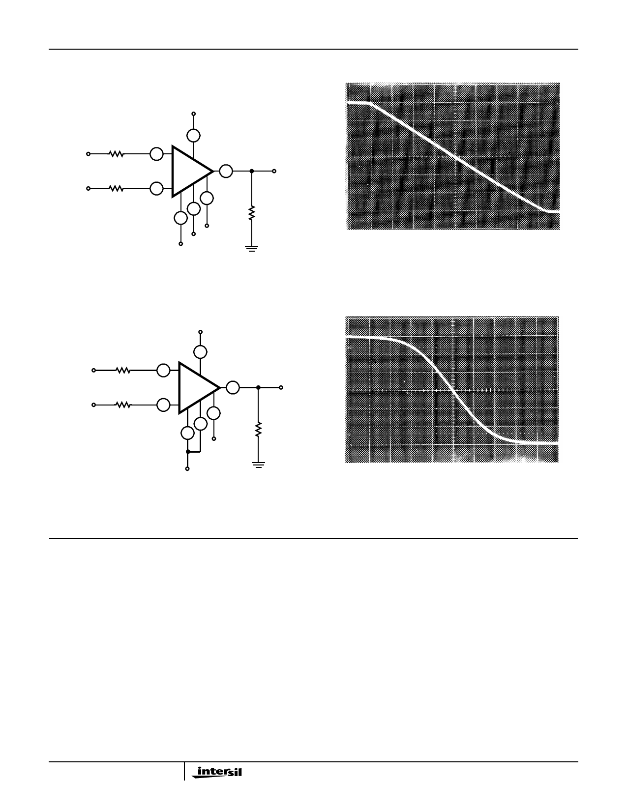
FIGURE 4. VOA SHOWING LINEARIZATION DIODES AND
CURRENT DRIVE
+15V
2kΩ
DIFFERENTIAL
INPUT 2kΩ
68kΩ
14
3
16 +
1/2
CA3280
13
15 -
4
1
SINGLE-
ENDED
OUTPUT
10kΩ
-15V
FIGURE 6. DIFFERENTIAL TO SINGLE ENDED CONVERTER
5
ID IABC
FIGURE 5. BLOCK DIAGRAM OF LINEARIZED VOA
10VP-P
INPUT
600Ω
10kΩ
V+
100kΩ
330kΩ
68kΩ
1
14
16 +
1/2
CA3280
15 -
4
V-
3
10kΩ
20kΩ
V+ = +15V
OUTPUT
21VP-P
14mV AGC
FEEDTHRU
400µV
NOISE AT
MAX GAIN
13
15kΩ
V- = -15V
VOLTAGE
CONTROL
FIGURE 7. TYPICAL GAIN CONTROL CIRCUIT
Share Link: 