WS7106CPL Ver la hoja de datos (PDF) - Wing Shing International Group
Número de pieza
componentes Descripción
Fabricante
WS7106CPL Datasheet PDF : 14 Pages
| |||
Differential Reference
The reference voltage can be generated anywhere within the
power supply voltage of the converter. The main source of com-
mon mode error is a roll-over voltage caused by the reference
capacitor losing or gaining charge to stray capacity on its
nodes. If there is a large common mode voltage, the reference
capacitor can gain charge (increase voltage) when called up to
de-integrate a positive signal but lose charge (decrease volt-
age) when called up to de-integrate a negative input signal.
This difference in reference for positive or negative input voltage
will give a roll-over error. However, by selecting the reference
capacitor such that it is large enough in comparison to the stray
capacitance, this error can be held to less than 0.5 count worst
case. (See Component Value Selection.)
Analog COMMON
This pin is included primarily to set the common mode
voltage for battery operation (WS7106) or for any system
where the input signals are floating with respect to the power
supply. The COMMON pin sets a voltage that is approxi-
mately 2.8V more negative than the positive supply. This is
selected to give a minimum end-of-life battery voltage of
about 6V. However, analog COMMON has some of the
attributes of a reference voltage. When the total supply
voltage is large enough to cause the zener to regulate (>7V),
the COMMON voltage will have a low voltage coefficient
(0.001%/V), low output impedance (≅15Ω), and a
temperature coefficient typically less than 80ppm/oC.
The limitations of the on chip reference should also be
recognized, however. With the WS7107, the internal heating
which results from the LED drivers can cause some
degradation in performance. Due to their higher thermal resis-
tance, plastic parts are poorer in this respect than ceramic.
The combination of reference Temperature Coefficient (TC),
internal chip dissipation, and package thermal resistance can
increase noise near full scale from 25µV to 80µVP-P. Also the
linearity in going from a high dissipation count such as 1000
(20 segments on) to a low dissipation count such as 1111(8
segments on) can suffer by a count or more. Devices with a
positive TC reference may require several counts to pull out of
an over-range condition. This is because over-range is a low
dissipation mode, with the three least significant digits
blanked. Similarly, units with a negative TC may cycle
between over-range and a non-over-range count as the die
alternately heats and cools. All these problems are of course
eliminated if an external reference is used.
The WS7106, with its negligible dissipation, suffers from
none of these problems. In either case, an external
reference can easily be added, as shown in Figure 4.
Analog COMMON is also used as the input low return during
auto-zero and de-integrate. If IN LO is different from analog
COMMON, a common mode voltage exists in the system
and is taken care of by the excellent CMRR of the converter.
However, in some applications IN LO will be set at a fixed
known voltage (power supply common for instance). In this
application, analog COMMON should be tied to the same
point, thus removing the common mode voltage from the
converter. The same holds true for the reference voltage. If
reference can be conveniently tied to analog COMMON, it
WS7106 / WS7107
should be since this removes the common mode voltage
from the reference system.
Within the lC, analog COMMON is tied to an N-Channel FET
that can sink approximately 30mA of current to hold the
voltage 2.8V below the positive supply (when a load is trying
to pull the common line positive). However, there is only
10µA of source current, so COMMON may easily be tied to a
more negative voltage thus overriding the internal reference.
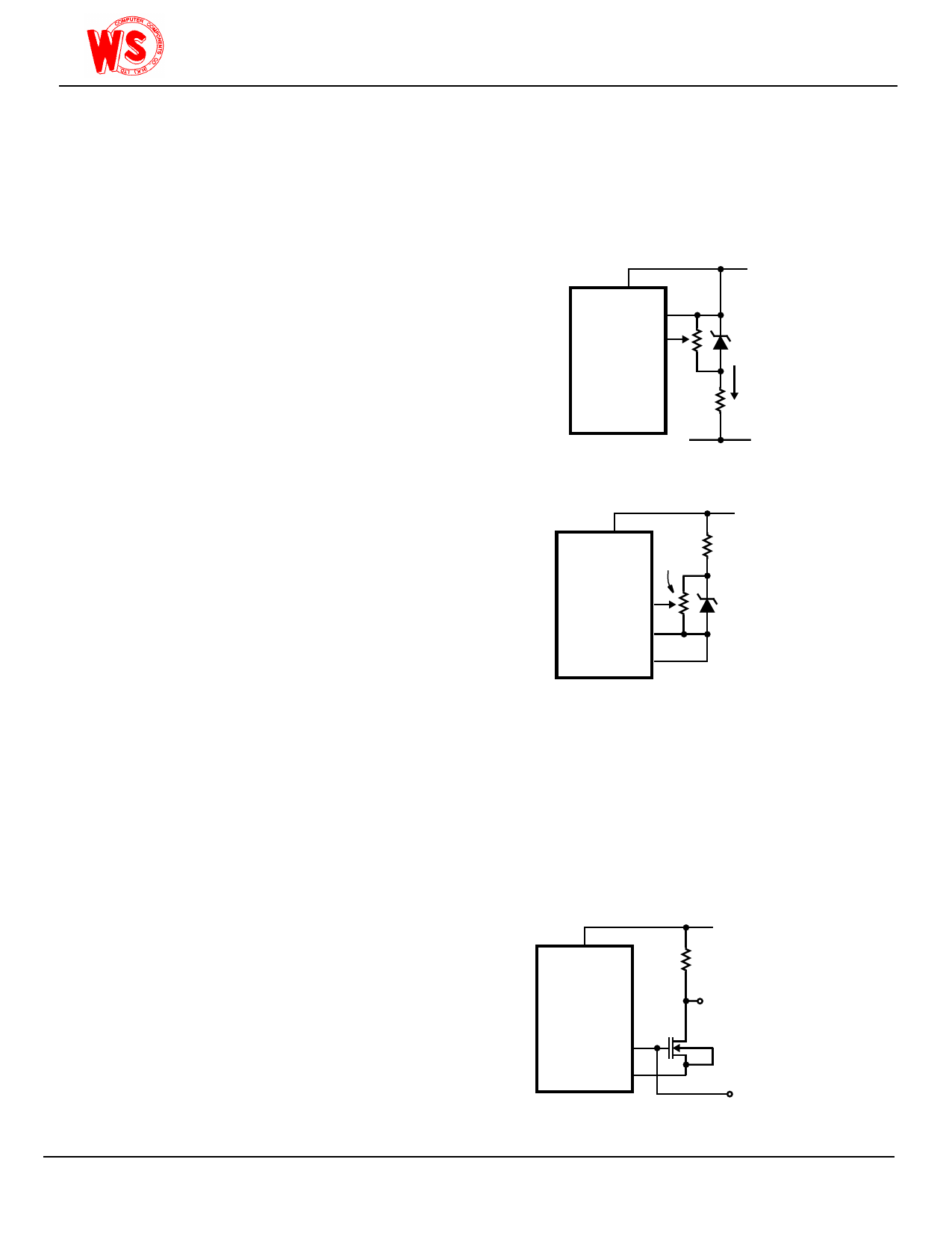
V+
V
REF HI
REF LO
WS7106
WS7107
6.8V
ZENER
IZ
V-
FIGURE 4A.
V+
V
WS7106
WS7107
REF HI
20kΩ
REF LO
COMMON
6.8kΩ
ICL8069
1.2V
REFERENCE
FIGURE 4B.
FIGURE 4. USING AN EXTERNAL REFERENCE
TEST
The TEST pin serves two functions. On the WS7106 it is
coupled to the internally generated digital supply through a
500Ω resistor. Thus it can be used as the negative supply for
externally generated segment drivers such as decimal points
or any other presentation the user may want to include on
the LCD display. Figures 5 and 6 show such an application.
No more than a 1mA load should be applied.
V+
1MΩ
WS7106
TO LCD
DECIMAL
POINT
BP 21
TEST
37
TO LCD
BACKPLANE
FIGURE 5. SIMPLE INVERTER FOR FIXED DECIMAL POINT
6
Share Link: 