WED9LC6816V1310BC Ver la hoja de datos (PDF) - White Electronic Designs => Micro Semi
Número de pieza
componentes Descripción
Fabricante
WED9LC6816V1310BC Datasheet PDF : 27 Pages
| |||
White Electronic Designs
WED9LC6816V
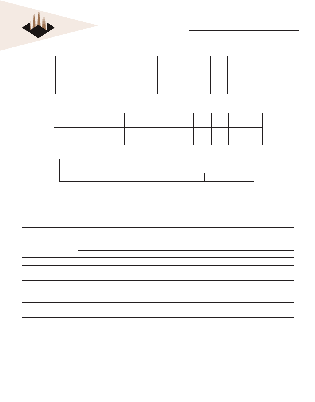
Clock Frequency and Latency Parameters - 125MHz SDRAM
(Unit = number of clock)
Frequency
LaCteAnScy
tRC
70ns
tRAS
50ns
tRP
20ns
tRRD
20ns
tRCD
20ns
tCCD
tCDL
10ns 10ns
tRDL
10ns
125MHz (8.0ns)
3
9
6
3
2
3
1
1
1
100MHz (10.0ns)
3
7
5
2
2
2
1
1
1
83MHz (12.0ns)
2
6
4
2
2
2
1
1
1
Clock Frequency and Latency Parameters - 100MHz SDRAM
(Unit = number of clock)
Frequency
CAS
Latency
tRC
70ns
tRAS
50ns
tRP
20ns
tRRD
20ns
tRCD
20ns
tCCD
10ns
tCDL
10ns
100MHz (12.0ns)
3
7
5
2
2
2
1
1
83MHz (12.0ns)
2
6
5
2
2
2
1
1
tRDL
10ns
1
Refresh Cycle Parameters
Parameter
Symbol
-10
Min
Max
-12
Min
Max
Units
Refresh Period (1,2)
tREF
—
64
—
64
ms
NOTES:
1. 4096 cycles
2. Any time that the Refresh Period has been exceeded, a minimum of two Auto (CBR) Refresh commands must be given to
"wake-up" the device.
SDRAM Command Truth Table
SDA10
Function
SDCE# SDRAS# SDCAS# SDWE # BWE# A12, A13
A11-0
Mode Register Set
L
L
L
L
X
OP CODE
Notes
Auto Refresh (CBR)
L
L
L
H
X
X
X
Precharge
Single Bank
L
L
H
L
X
BA
L
2
Precharge all Banks
L
L
H
L
X
X
H
Bank Activate
L
L
H
H
X
BA
Row Address
2
Write
L
H
L
L
X
BA
L
2
Write with Auto Precharge
L
H
L
L
X
BA
H
2
Read
L
H
L
L
X
BA
L
2
Read with Auto Precharge
L
H
L
H
X
BA
H
2
Burst Termination
L
H
H
L
X
X
X
3
No Operation
L
H
H
H
X
X
X
Device Deselect
H
X
X
X
X
X
X
Data Write/Output Disable
X
X
X
X
L
X
X
4
Data Mask/Output Disable
X
X
X
X
H
X
X
4
NOTES:
1. All of the SDRAM operations are defined by states of SDCE#, SDWE#, SDRAS#, SDCAS#, and BWE0-3# at the positive rising edge of the clock.
2. Bank Select (BA), A12 (BA0) and A13 (BA1) select between different banks.
3. During a Burst Write cycle there is a zero clock delay, for a Burst Read cycle the delay is equal to the CAS latency.
4. The BWE# has two functions for the data DQ Read and Write operations. During a Read cycle, when BWE# goes high at a clock timing the data outputs are disabled
and become high impedance after a two clock delay. BWE# also provides a data mask function for Write cycles. When it activates, the Write operation at the clock is
prohibited (zero clock latency).
Contact factory for ordering information.
White Electronic Designs Corp. reserves the right to change products or specifications without notice.
September, 2003
Rev. 1
9
White Electronic Designs Corporation • (602) 437-1520 • www.wedc.com
Share Link: 