VT98521/DW Ver la hoja de datos (PDF) - Vaishali Semiconductor
Número de pieza
componentes Descripción
Fabricante
VT98521/DW Datasheet PDF : 5 Pages
| |||
Applications
•= Low cost general-purpose clock source
VT98521
3.3V Clock Multiplier
General Description
The VT98521 is a 3.3V CMOS, clock multiplier integrated circuit. The device provides an excellent quality
high frequency output clock from a lower frequency crystal or clock input. Tri-level selection inputs S0 and
S1 are used to select any one of eight multipliers, stored in the on-board ROM, and apply it to the input to
produce the desired output, up to 220 MHz. Phase Locked Loop (PLL) technology allows the device to use
an input signal from an inexpensive crystal. When Output Enable (OE) is low, the clock output is in high
impedance state.
The VT98521, when used with an inexpensive crystal, provides a cost-effective clock source for most
electronic systems.
Features
•= Low phase noise
•= Zero ppm multiplication error
•= Input clock frequency 5 - 50 MHz.
•= Input crystal frequency 5 – 27 MHz
•= Output clock frequencies up to 220 MHz.
•= 5V-tolerant inputs and output
•= Fully Compatible with all popular CPUs
•= Duty Cycle - 45/55 up to 160 MHz.
- 40/60 160 MHz to 220 MHz
•= 25mA drive capability at TTL levels
•= High-Z output for board level testing
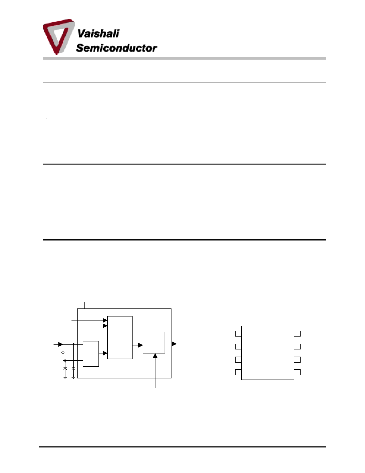
Figure 1. Functional Block Diagram
Figure 2. Pin Assignment
VDD
GND
S0
S1
Clock or
Xtal
input
X1/ICLK
Xtal.
Osc.
X2
PLL
Clock
Multiplier
&
ROM
Output
CLK
Buffer
Optional
caps
Output Enable
8-pin SOIC/MSOP
X1/ICLK
1
VDD
2
GND
3
S1
4
8
X2
7
OE
6
S0
5
CLK
2002-02-25
Vaishali Semiconductor
Page 1
www.vaishali.com
747 Camden Avenue, Suite C Campbell
CA 95008
Ph. 408.377.6060
MDST-0017-02
Fax 408.377.6063
Share Link: 