BUL642D2 Ver la hoja de datos (PDF) - ON Semiconductor
Número de pieza
componentes Descripción
Fabricante
BUL642D2 Datasheet PDF : 8 Pages
| |||
BUL642D2
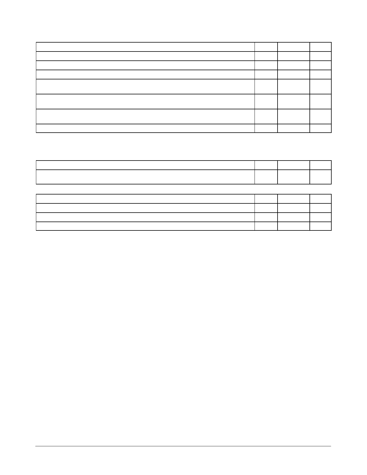
MAXIMUM RATINGS
Rating
Symbol
Value
Unit
Collector−Emitter Sustaining Voltage
Collector−Base Breakdown Voltage
Emitter−Base Voltage
Collector Current − Continuous
− Peak (Note 1)
Base Current
− Continuous
− Peak (Note 1)
*Total Device Dissipation @ TC = 25°C
*Derate above 25°C
VCEO
VCES
VEBO
IC
ICM
IB
IBM
PD
440
Vdc
825
Vdc
11
Vdc
3.0
Adc
8.0
2.0
Adc
4.0
75
W
0.6
W/°C
Operating and Storage Temperature
TJ, Tstg − 65 to +150 °C
Maximum ratings are those values beyond which device damage can occur. Maximum ratings applied to the device are individual stress limit
values (not normal operating conditions) and are not valid simultaneously. If these limits are exceeded, device functional operation is not implied,
damage may occur and reliability may be affected.
TYPICAL GAIN
Rating
Symbol
Value
Unit
Typical Gain @ IC = 1 A, VCE = 2 V
Typical A, VCE = 1 V
THERMAL CHARACTERISTICS
hFE
45
−
hFE
50
−
Characteristic
Symbol
Value
Unit
Thermal Resistance, Junction−to−Case
Thermal Resistance, Junction−to−Ambient
Maximum Lead Temperature for Soldering Purposes: 1/8 in. from Case for 5 seconds
1. Pulse Test: Pulse Width = 5.0 ms, Duty Cycle = 10%
RqJC
RqJA
TL
1.6
°C/W
62.5
°C/W
260
°C
http://onsemi.com
2
Share Link: 