AS4LC1M16S1-10TC Ver la hoja de datos (PDF) - Alliance Semiconductor
NГәmero de pieza
componentes DescripciГіn
Fabricante
AS4LC1M16S1-10TC Datasheet PDF : 28 Pages
| |||
AS4LC2M8S1
AS4LC1M16S1
Functional description
The AS4LC2M8S1 and AS4LC1M16S1 are high-performance 16-megabit CMOS Synchronous Dynamic Random Access Memory (SDRAM)
devices organized as 1,048,576 words Г— 8 bits Г— 2 banks (2048 rows Г— 512 columns) and 524,288 words Г— 16 bits Г— 2 banks
(2048 rows Г— 256 columns), respectively. Very high bandwidth is achieved using a pipelined architecture where all inputs and outputs are
referenced to the rising edge of a common clock. Programmable burst mode can be used to read up to a full page of data (512 bytes for
2M Г— 8 and 256 bytes for 1M Г— 16) without selecting a new column address.
The operational advantages of an SDRAM are as follows: (1) the ability to synchronously output data at a high clock frequency with
automatic increments of column-address (burst access); (2) bank-interleaving, which hides precharge time and attains seamless op eration;
and (3) the capability to change column-address randomly on every clock cycle during burst access.
This SDRAM product also features a programmable mode register, allowing users to select read latency as well as burst length and type
(sequential or interleaved). Lower latency improves first data access in terms of CLK cycles, while higher latency improves maximum
frequency of operation. This feature enables flexible performance optimization for a variety of applications.
SDRAM commands and functions are decoded from control inputs. Basic commands are as follows:
вҖў Mode register set
вҖў Deactivate bank
вҖў Deactivate all banks
вҖў Select column; write
вҖў Select column; read
вҖў Deselect; power down
вҖў Auto precharge with read/write вҖў Self-refresh
вҖў Select row; activate bank
вҖў CBR refresh
Both devices are available in 400-mil plastic TSOP type 2 package. The AS4LC2M8S1 has 44 pins, and the AS4LC1M16S1 has 50 pins. Both
devices operate with a power supply of 3.3V Вұ 0.3V. Multiple power and ground pins are provided for low switching noise and EMI. Inputs
and outputs are LVTTL compatible.
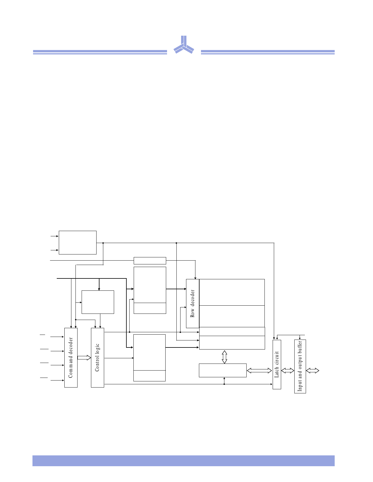
Logic block diagram
CLK
Clock generator
CKE
A11
Bank select
A[10:0]
CS
RAS
CAS
WE
Mode register
Row
address
buffer
Refresh
counter
Column
address
buffer
Burst
counter
Bank AвҖ
512K Г— 16 (2048 Г— 256 Г— 16)
Bank BвҖ
512K Г— 16 (2048 Г— 256 Г— 16)
Sense amplifier
Column decoder and
latch circuit
Data control circuit
DQMU/DQML
DQ
вҖ For AS4LC2M8S1, Banks A and B will read 1M Г— 8 (2048 Г— 512 Г— 8).
2
ALLIANCE SEMICONDUCTOR
7/5/00
Share Link: 