BD9892K Ver la hoja de datos (PDF) - ROHM Semiconductor
Número de pieza
componentes Descripción
Fabricante
BD9892K Datasheet PDF : 5 Pages
| |||
4/4
〇NOTE FOR USE
1. When designing the external circuit, including adequate margins for variation between external devices and the IC.Use
adequate margins for steady state and transient characteristics.
2. Recommended Operating Range
The circuit functionality is guaranteed within of ambient temperature operation range as long as it is within recommended
operating range. The standard electrical characteristic values cannot be guaranteed at other voltages in the operating
ranges, however, the variation will be small.
3. Mounting Failures
Mounting failures, such as misdirection or miscounts, may harm the device.
4. Electromagnetic Fields
A strong electromagnetic field may cause the IC to malfunction.
5. The GND pin should be the location within ±0.3V compared with the PGND(A,B) pin
6. BD9892K has the short circuit protection with Thermal Shut Down System. When STB or Vcc pin re-supplied, They enables
to cancel the latch. If It rise the temperature of the chip more than 170℃(TYP), It make the external FET OFF
7. Absolute maximum ratings are those values that, if exceeded, may cause the life of a device to become significantly shortened.
Moreover, the exact failure mode caused by short or open is not defined. Physical countermeasures, such as a fuse, need
to be considered when using a device beyond its maximum ratings.
8. About the external FET, the parasitic Capacitor may cause the gate voltage to change, when the drain voltage is switching.
Make sure to leave adequate margin for this IC variation.
9. On operating Slow Start Control (SS(A,B) is less than 2.2V), It does not operate Timer Latch.
10. By STB voltage, BD9892K is changed to 2 states. Therefore, do not input STB pin voltage between one state and the other
state (0.8~2.0).
11.The pin connected a connector need to connect to the resistor for electrical surge destruction.
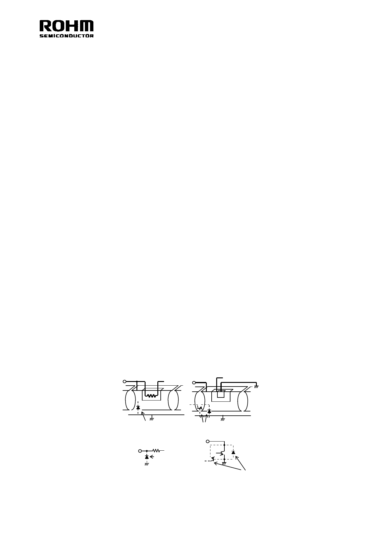
12.This IC is a monolithic IC which (as shown is Fig-1)has P+ substrate and between the various pins. A P-N junction is
formed from this P layer of each pin. For example, the relation between each potential is as follows,
○(When GND > PinB and GND > PinA, the P-N junction operates as a parasitic diode.)
○(When PinB > GND > PinA, the P-N junction operates as a parasitic transistor.)
Parasitic diodes can occur inevitably in the structure of the IC. The operation of parasitic diodes can result in mutual
interference among circuits as well as operation faults and physical damage. Accordingly you must not use methods by which
parasitic diodes operate, such as applying a voltage that is lower than the GND(P substrate)voltage to an input pin.
Resistance
Transistor (NPN)
(PinA)
P+
N
P
P+
N
P substrate
GND
Parasitic diode
(PinB)
B
CC
E
GND
N
N
N
N
P substrate
GND
Parasitic diode
(PinB)
(PinA)
Parasitic diode
B BC C
EE
GND
GND
Other adjacent components Parasitic diode
Fig.1 Simplified structure of a Bipolar IC
REV. B
Share Link: 