BD6373GW Ver la hoja de datos (PDF) - ROHM Semiconductor
Número de pieza
componentes Descripción
Fabricante
BD6373GW
ROHM Semiconductor

BD6373GW Datasheet PDF : 18 Pages
| |||
BD6373GW, BD6873KN, BD6753KV
Bypass filter Capacitor for
power supply input. (p.14/16)
Power-saving (p.8/16)
H : Active
L : Standby
Motor control input
(p.8/16)
Drive mode selection
(p.8/16)
H : EN/IN
L : IN/IN
Motor control input
(p.8/16)
Drive mode selection
(p.8/16)
H : EN/IN
L : IN/IN
Motor control input
(p.8/16)
Drive mode selection
(p.8/16)
H : EN/IN
L : IN/IN
Motor control input
brake function (p.8/16)
H : Brake
PS 38
IN1A 47
IN1B 48
IN2A 1
IN2B 2
SEL1 3
IN3A 4
IN3B 5
IN4A 8
IN4B 9
SEL2 10
IN5A 11
IN5B 12
SEL3 13
BRK1 14
Power Save
Logic12
Logic34
Logic5
1~100uF
VCC
6
TSD & UVLO
Level Shift
&
Pre Driver
Level Shift
&
Pre Driver
Level Shift
&
Pre Driver
BandGap
H bridge
Full ON
H bridge
Full ON
H bridge
Full ON
H bridge
Full ON
H bridge
Full ON
Motor control input
(p.8/16)
EN1 36
IN6 37
Logic6
VREF
Level Shift
&
Pre Driver
Selector
H bridge
Const. Current
When using the VREF voltage (1.2V) resistance division
value as VLIMH and VLIML input value, select R1, R2, and R3
values such that,
2kΩ≦R1+R2+R3≦20kΩ (p.9/16)
23
26
VREF
VLIMS
24
25
VLIMH VLIML
R1
R2
R3
7
GND
Output current selection
(p.10/16)
H : VLIML
L : VLIMH
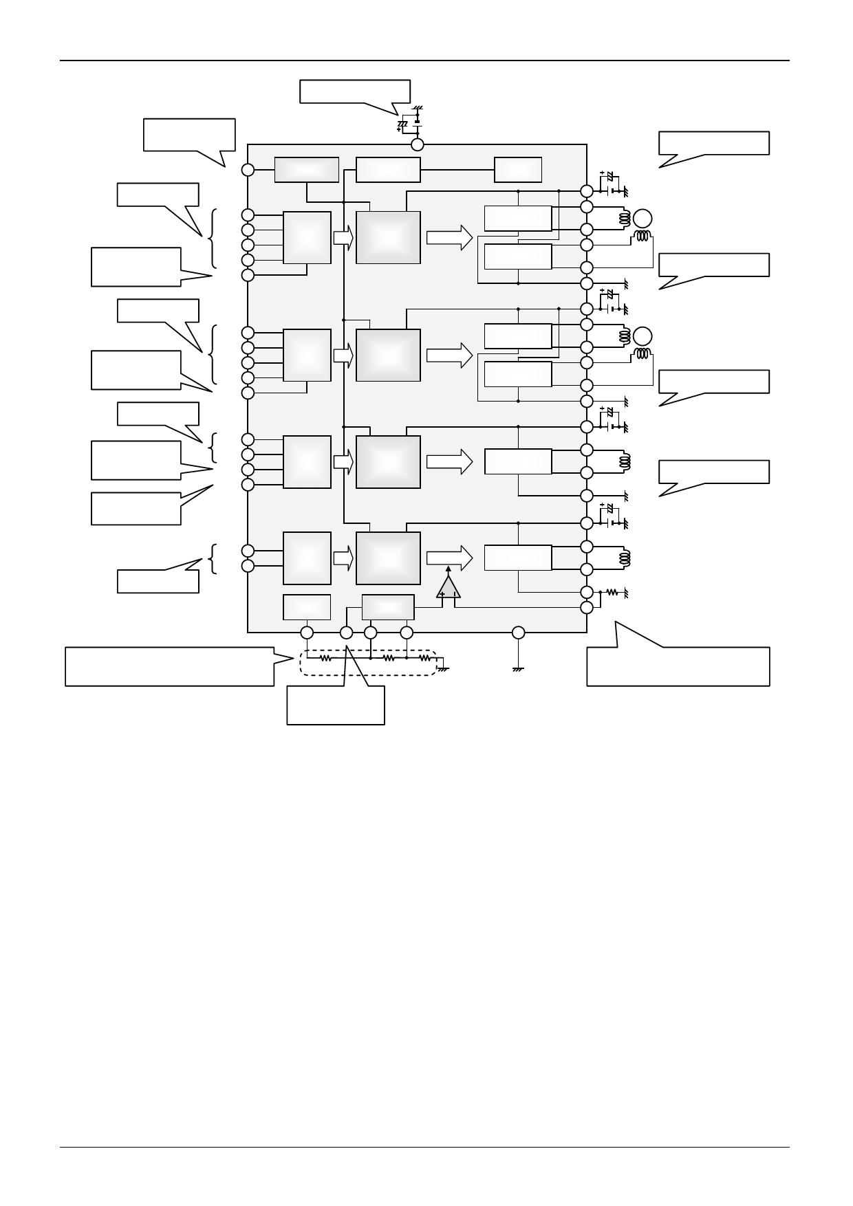
Fig.19 BD6873KN Application Circuit Diagram
Technical Note
Bypass filter Capacitor for
power supply input. (p.14/16)
1~100uF
41
VM1
39 OUT1A
M
40 OUT1B
45 OUT2A
46 OUT2B
44 PGND1
1~100uF
17
VM2
15 OUT3A
M
16 OUT3B
21 OUT4A
22 OUT4B
20 PGND2
1~100uF
34
VM3
32 OUT5A
35 OUT5B
33 PGND3
1~100uF
28
VM4
27
OUT6A
31 OUT6B
RNF
29
30
0.1Ω~5.0Ω
SENSE
Bypass filter Capacitor for
power supply input. (p.14/16)
Bypass filter Capacitor for
power supply input. (p.14/16)
Bypass filter Capacitor for
power supply input. (p.14/16)
The output current is converted to a voltage with
the RNF external resistor and transmitted to the
SENSE pin. (p.10/16)
Iout[A] = (VLIMH or VLIML[V])÷RNF[Ω]
3) H-bridge
The 6-channel H-bridges of can be controlled independently. For this reason, it is possible to drive the H-bridges
simultaneously, as long as the package thermal tolerances are not exceeded.
The H-bridge output transistors of the BD6373GW, BD6873KN and BD6753KV consist of Power CMOS, with the motor
power supply VM, and Power DMOS, with the charge pump step-up power supply VG, respectively. The total H-bridge
ON-Resistance on the high and low sides varies with the VM and VG voltages, respectively. The system must be
designed so that the maximum H-bridge current for each channel is 800mA or below.
4) Drive system of Linear Constant-Current H-bridge (BD6873KN: ch6)
BD6873KN (ch6) enables Linear Constant-Current Driving.
(1) Reference voltage output (with a tolerance of ±3%)
The VREF pin outputs 1.2V, based on the internal reference voltage. The output current of the Constant-Current Drive
block is controllable by connecting external resistance to the VREF pin of the IC and applying a voltage divided by the
resistor to the output current setting pins (VLIMH and VLIML pins). It is recommended to set the external resistance to
2kΩ or above in consideration of the current capacity of the VREF pin, and 20kΩ or below in order to minimize the
fluctuation of the set value caused by the base current of the internal transistor of the IC.
www.rohm.com
© 2009 ROHM Co., Ltd. All rights reserved.
9/17
2009.06 - Rev.A
Share Link: