BD6373GW Ver la hoja de datos (PDF) - ROHM Semiconductor
Número de pieza
componentes Descripción
Fabricante
BD6373GW
ROHM Semiconductor

BD6373GW Datasheet PDF : 18 Pages
| |||
BD6373GW, BD6873KN, BD6753KV
Technical Note
PS 38
Power Save
VCC
6
TSD & UVLO
IN1A 47
IN1B 48
IN2A 1
IN2B 2
SEL1 3
Logic12
Level Shift
&
Pre Driver
BandGap
H bridge
Full ON
H bridge
Full ON
41 VM1
39 OUT1A
40 OUT1B
45 OUT2A
46 OUT2B
44 PGND1
IN3A 4
IN3B 5
IN4A 8
IN4B 9
SEL2 10
Logic34
IN5A 11
IN5B 12
SEL3 13
BRK1 14
Logic5
Level Shift
&
Pre Driver
Level Shift
&
Pre Driver
H bridge
Full ON
H bridge
Full ON
H bridge
Full ON
EN1 36
IN6 37
Logic6
Level Shift
&
Pre Driver
H bridge
Const. Current
VREF
Selector
23
26
VREF
VLIMS
24
25
VLIMH VLIML
7
GND
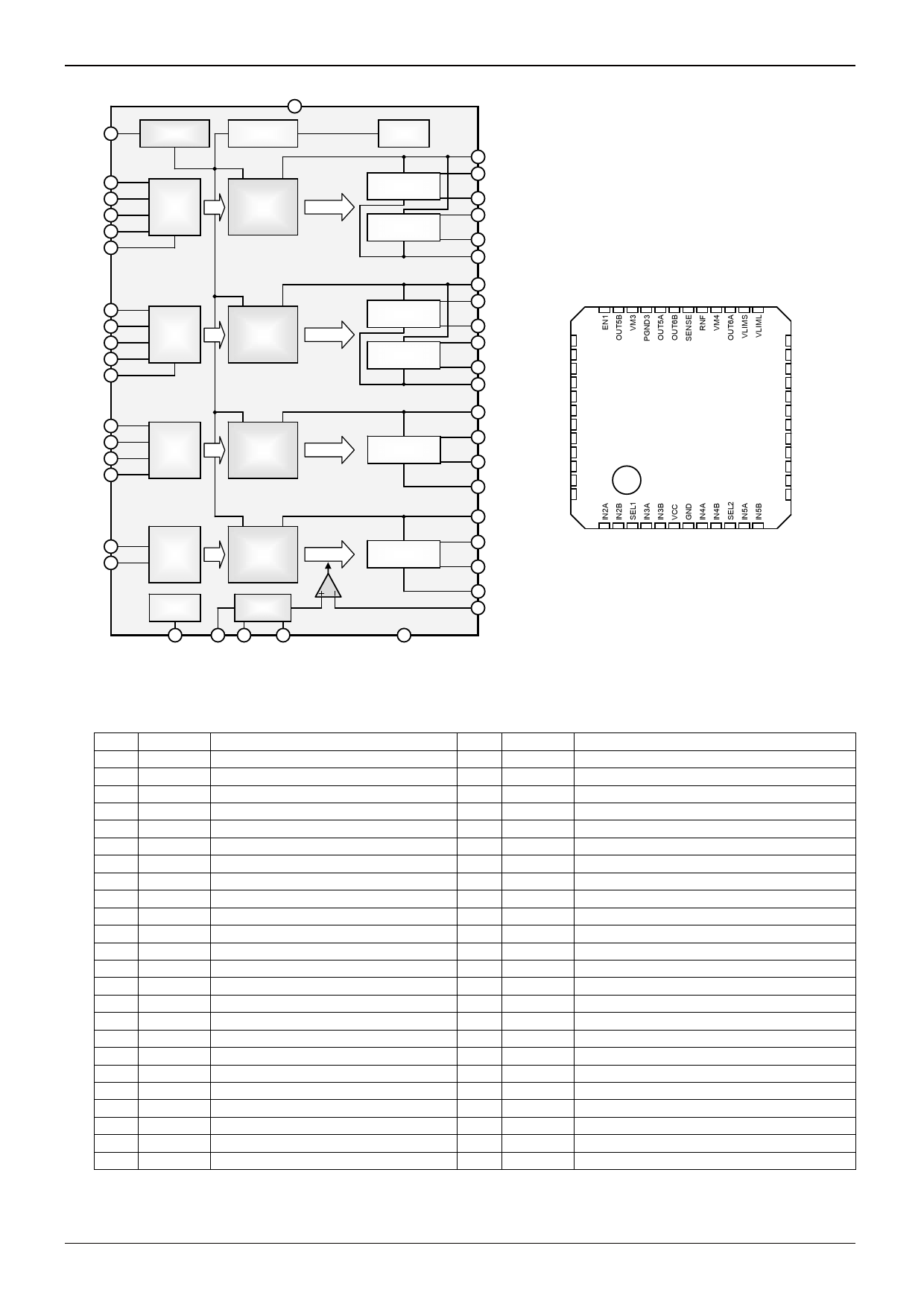
Fig.14 BD6873KN Block Diagram
17 VM2
15 OUT3A
16 OUT3B
21 OUT4A
22 OUT4B
20 PGND2
34 VM3
32 OUT5A
35 OUT5B
33 PGND3
28 VM4
27 OUT6A
31 OUT6B
29 RNF
30 SENSE
36
IN6
PS
OUT1A
OUT1B
VM1
N.C.
N.C.
PGND1
OUT2A
OUT2B
IN1A
48 IN1B
BD6873KN
VLIMH 24
VREF
OUT4B
OUT4A
PGND2
N.C.
N.C.
VM2
OUT3B
OUT3A
BRK1
SEL3
12
Fig.15 BD6873KN Pin Arrangement (Top View)
UQFN48 Package
BD6873KN Pin Function Table
No. Pin name
Function
No. Pin name
Function
1
IN2A Control input pin ch2 A
25 VLIML Output current setting pin 2 ch6
2
IN2B Control input pin ch2 B
26 VLIMS Output current selection pin ch6
3
SEL1 Input mode selection pin ch1 and ch2 27 OUT6A H-bridge output pin ch6 A
4
IN3A Control input pin ch3 A
28
VM4 Motor power supply pin ch6
5
IN3B Control input pin ch3 B
29
RNF
Resistance connection pin for output current detection ch6
6
VCC Power supply pin
30 SENSE Output current detection pin ch6
7
GND Ground pin
31 OUT6B H-bridge output pin ch6 B
8
IN4A Control input pin ch4 A
32 OUT5A H-bridge output pin ch5 A
9
IN4B Control input pin ch4 B
33 PGND3 Motor ground pin ch5
10 SEL2 Input mode selection pin ch3 and ch4 34
VM3 Motor power supply pin ch5
11
IN5A Control input pin ch5 A
35 OUT5B H-bridge output pin ch5 B
12
IN5B Control input pin ch5 B
36
EN1 Control input pin ch6 ENABLE
13 SEL3 Input mode selection pin ch5
37
IN6 Control input pin ch6 INPUT
14 BRK1 Control input pin ch5 BRAKE
38
PS Power-saving pin
15 OUT3A H-bridge output pin ch3 A
39 OUT1A H-bridge output pin ch1 A
16 OUT3B H-bridge output pin ch3 B
40 OUT1B H-bridge output pin ch1 B
17
VM2 Motor power supply pin ch3 and ch4 41
VM1 Motor power supply pin ch1 and ch2
18
N.C.
-
42
N.C.
-
19
N.C.
-
43
N.C.
-
20 PGND2 Motor ground pin ch3 and ch4
44 PGND1 Motor ground pin ch1 and ch2
21 OUT4A H-bridge output pin ch4 A
45 OUT2A H-bridge output pin ch2 A
22 OUT4B H-bridge output pin ch4 B
46 OUT2B H-bridge output pin ch2 B
23 VREF Reference voltage output pin
47
IN1A Control input pin ch1 A
24 VLIMH Output current setting pin 1 ch6
48
IN1B Control input pin ch1 B
www.rohm.com
© 2009 ROHM Co., Ltd. All rights reserved.
6/17
2009.06 - Rev.A
Share Link: