BD6373GW Ver la hoja de datos (PDF) - ROHM Semiconductor
Número de pieza
componentes Descripción
Fabricante
BD6373GW
ROHM Semiconductor

BD6373GW Datasheet PDF : 18 Pages
| |||
BD6373GW, BD6873KN, BD6753KV
Technical Note
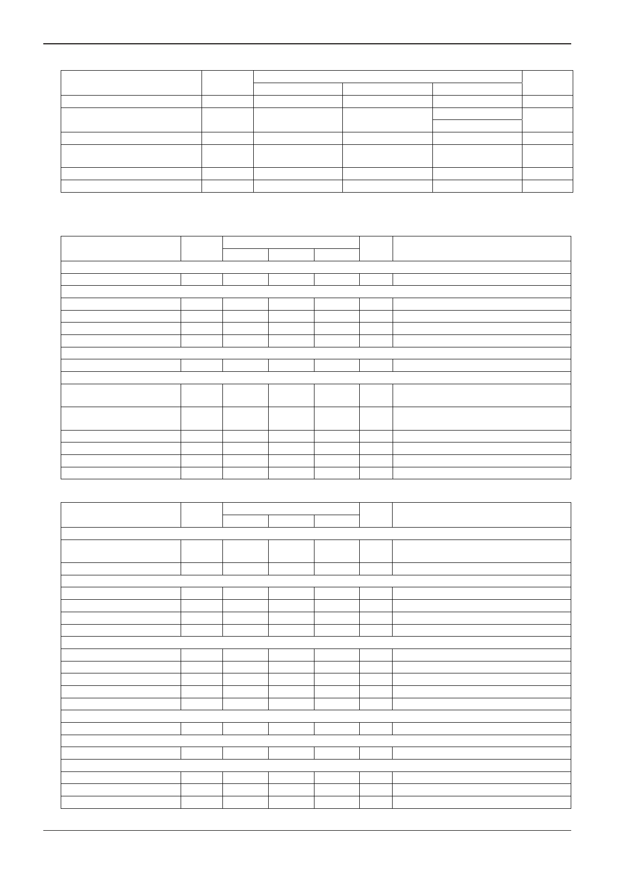
●Operating Conditions (Ta=-25 to +85°C(BD6373GW, BD6873KN), -25 to +75°C(BD6753KV))
Parameter
Symbol
BD6373GW
Limit
BD6873KN
BD6753KV
Power supply voltage
VCC
2.5 to 5.5
2.5 to 5.5
2.7 to 5.5
Motor power supply voltage
VM
2.5 to 5.5
2.5 to 5.5
4.5 to 10.5 (VM1)
2.0 to 10.5 (VM2 to VM4)
Control input voltage
VIN
0 to VCC
0 to VCC
0 to VCC
Output current control input
voltage range
VLIM
-
0 to VCC
0 to 0.5
PWM signal input frequency
H-bridge output current
FPWM
Iout
-
-500 to +500※5
-
-500 to +500※5
0 to 0.1
-500 to +500※5
※5 Must not exceed Pd or ASO.
Unit
V
V
V
V
MHz
mA/ch
●Electrical Characteristics
1) BD6373GW Electrical Characteristics (Unless otherwise specified, Ta=25°C, VCC=3.0V, VM=5.0V)
Parameter
Symbol Min.
Limit
Typ.
Max.
Unit
Conditions
Overall
Circuit current
ICC
-
1.0
1.9
mA no signal and no load
Control input (IN=ENABLExx, INPUTx, and BRAKEx)
High level input voltage
VINH
2.0
-
VCC
V
Low level input voltage
VINL
0
-
0.7
V
High level input current
IINH
15
30
60
μA VINH=3V
Low level input current
IINL
-1
0
-
μA VINL=0V
UVLO
UVLO voltage
VUVLO 1.6
-
2.4
V
Full-ON Drive block (ch1 to ch6)
Output ON-Resistance 1
RON1
-
1.2
1.5
Ω
Io=±400mA on high and low sides In total
(VM=5V)
Output ON-Resistance 2
RON2
-
1.5
2.0
Ω
Io=±400mA on high and low sides In total
(VM=3V)
Turn on time
ton
-
0.55
1.95
μs RL=20Ω
Turn off time
toff
-
0.08
0.5
μs RL=20Ω
Rise time
tr
0.1
0.15
1.0
μs RL=20Ω
Fall time
tf
-
0.03
0.2
μs RL=20Ω
2) BD6873KN Electrical Characteristics (Unless otherwise specified, Ta=25°C, VCC=3.0V, VM=5.0V)
Parameter
Symbol Min.
Limit
Typ.
Max.
Unit
Conditions
Overall
Circuit current
during standby operation
ICCST
-
0
10
μA PS=0V
Circuit current
ICC
-
1.2
2.3
mA PS=VCC with no signal and no load
Power-saving (PS)
High level input voltage
VPSH
2.0
-
-
V
Low level input voltage
VPSL
-
-
0.7
V
High level input current
IPSH
15
30
60
μA VPS=3V
Low level input current
IPSL
-1
0
-
μA VPS=0V
Control input (IN=IN1A to IN5B, SEL1 to 3, BRK1, EN1, IN6, and VLIMS)
High level input voltage
VINH
2.0
-
-
V
Low level input voltage
VINL
-
-
0.7
V
High level input current
IINH
15
30
60
μA VINH=3V
Low level input current
IINL
-1
0
-
μA VINL=0V
Pull-down resistance
RIN
50
100
200
kΩ
UVLO
UVLO voltage
VUVLO 1.6
-
2.4
V
Full-ON Drive block (ch1 to ch5)
Output ON-Resistance
RON
-
1.2
1.5
Ω Io=±400mA on high and low sides In total
Linear Constant-Current Drive block (ch6)
Output ON-Resistance
RON
-
1.0
1.25
Ω Io=±400mA on high and low sides in total
VREF output voltage
VREF 1.16
1.20
1.24
V Iout=0~1mA
Output limit voltage
VOL
194
200
206
mV RNF=0.5Ω, VLIM=0.2V
www.rohm.com
© 2009 ROHM Co., Ltd. All rights reserved.
2/17
2009.06 - Rev.A
Share Link: