BD6373GW Ver la hoja de datos (PDF) - ROHM Semiconductor
Número de pieza
componentes Descripción
Fabricante
BD6373GW
ROHM Semiconductor

BD6373GW Datasheet PDF : 18 Pages
| |||
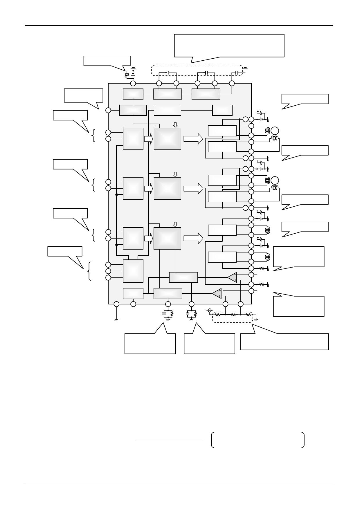
BD6373GW, BD6873KN, BD6753KV
Technical Note
Bypass filter Capacitor for
power supply input. (p.14/16)
Power-saving (p.8/16)
H : Active
L : Standby
1~100uF
VCC
9
OSC
Motor control input
(p.8/16)
PS 28
Power Save
PWM1 2
PWM2 3
Logic12
Motor control input
(p.8/16)
PWM3 10
PWM4 11
Logic34
Motor control input
(p.8/16)
Serial control input
(p.12/16)
PWM5 12
PWM6 1
Logic4556
STROBE 31
CLK 32
DATA 33
Serial
Interface
VREF
30
GND
29
VREF
Connecting 0.01μF to 0.1μF capacitors between the CP1 and CP2, CP3
and CP4, and VG and GND pins generate a VG voltage of approximately
VM1 + (VCC 2). Use caution to ensure that the voltage differential between
VG and VM is 4.5V or higher, and that the VG voltage does not exceed the
absolute maximum rating of 18V, especially BST voltage direct input.
(p.12/16)
0.1μF
0.1μF
0.1μF
CP1
4
CP2
5
CP3
6
CP4
7
VG
8
Charge Pump
Charge Pump
Bypass filter Capacitor for
power supply input. (p.14/16)
TSD & UVLO
VG
L
VG
L
VG
L
PWM LATCH
PWM LATCH
27
CR1
34
CR2
CCR1
RCR1 CCR2
RCR2
BandGap
1~100uF
H bridge
Full ON
44 45
VM1
41 OUT1A
M
43 OUT1B
H bridge
Full ON
46 OUT2A
48 OUT2B
42 47 RNF1
1~100uF
Bypass filter Capacitor for
power supply input. (p.14/16)
H bridge
Full ON
16 17
VM2
13
OUT3A
M
15 OUT3B
H bridge
Full ON
18 OUT4A
20 OUT4B
14 19 RNF2
1~100uF
Bypass filter Capacitor for
power supply input. (p.14/16)
H bridge
PWM C. Current
25
VM3
21 OUT5A
24 OUT5B
1~100uF
Bypass filter Capacitor for
power supply input. (p.14/16)
H bridge
PWM C. Current
36
VM4
37 OUT6A
40 OUT6B
RNF4
39
38 0.1Ω~5.0Ω
SENSE4
RNF3
22
23
0.1Ω~5.0Ω
SENSE3
26
35
VREF VLIM5 VLIM6
R1
R2
R3
The output current is converted
to a voltage with the RNF4
external resistor and transmitted
to the SENSE4 pin. (p.11/16)
Iout[A] = VLIM6[V]÷RNF4[Ω]
The output current is converted
to a voltage with the RNF3
external resistor and transmitted
to the SENSE3 pin. (p.11/16)
Iout[A] = VLIM5[V]÷RNF3[Ω]
This CR timer determines the
off time for the PWM drive.
5kΩ≦RCR1≦50kΩ
10pF≦CCR1≦2200pF
(p.11/16)
This CR timer determines the
off time for the PWM drive.
5kΩ≦RCR2≦50kΩ
10pF≦CCR2≦2200pF
(p.11/16)
When using the VREF voltage (0.9V) resistance division
value as VLIM5 and VLIM6 input value, select R1, R2, and R3
values such that,
1kΩ≦R1+R2+R3≦20kΩ (p.11/16)
Fig.20 BD6753KV Application Circuit Diagram
(2) Output current settings and setting changes
When the Low-level control voltage is applied to the VLIMS pin, the value on the VLIMH pin will be used as an output current
set value to control the output current. When the High-level control voltage is applied to the VLIMS pin, the value on the VLIML
pin will be used as an output current set value to control the output current. (See the Electrical Characteristics; P.2/16)
(3) Output current detection and current settings
By connecting external resistor (0.1Ω to 5.0Ω) to the RNF pin of the IC, the motor drive current will be converted into voltage in
order to be detected. The output current is kept constant by shorting the RNF and SENSE pins and comparing the voltage with
the VLIMH or VLIML voltage. To perform output current settings more precisely, trim the external RNF resistance if needed, and
supply a precise voltage externally to the VLIMH or VLIML pin of the IC. In that case, open the VREF pin.
Output current value Iout[A] =
VLIMH[V] or VLIML[V]
RNF[Ω]
Select VLIMH when VLIMS is Low-level
Select VLIML when VLIMS is High-level
・・・・・・(1)
The output current is 400mA3% if 0.2V is applied to the VLIMH or VLIML pin and a 0.5Ω resistor is connected externally to
the RNF pin.
If the VLIMH and VLIML pins are shorted to the VCC pin (or the same voltage level as the VCC is applied) and the SENSE and
RNF pins are shorted to the ground, this channel can be used as a Full-ON Drive H-bridge like the other five channels.
www.rohm.com
© 2009 ROHM Co., Ltd. All rights reserved.
10/17
2009.06 - Rev.A
Share Link: