AZ100EL16VOL(2003) Ver la hoja de datos (PDF) - Arizona Microtek, Inc
Número de pieza
componentes Descripción
Fabricante
AZ100EL16VOL Datasheet PDF : 12 Pages
| |||
AZ10EL16VO
AZ100EL16VO
ARIZONA MICROTEK, INC.
ECL/PECL Oscillator Gain Stage and Buffer with Enable
FEATURES
• 250ps Propagation Delay on Q¯ Output
• High Voltage Gain vs. Standard EL16
• For Oscillator Applications
• Operating Range of 3.0V to 5.5V
• Available in 2x2 or 3x3mm MLP Package
• 75kΩ Enable Pull-Down Resistor
DESCRIPTION
PACKAGE AVAILABILITY
PACKAGE
MLP 8 (2x2x0.75)
MLP 8 (2x2x0.75)
T&R
MLP 8 (2x2x0.75)
T&R
MLP 16
MLP 16 T&R
MLP 16 T&R
SOIC 8
SOIC 8 T&R
SOIC 8 T&R
SOIC 8
SOIC 8 T&R
SOIC 8 T&R
TSSOP 8
TSSOP 8 T&R
TSSOP 8 T&R
TSSOP 8
TSSOP 8
TSSOP 8 T&R
TSSOP 8 T&R
DIE
PART NO.
AZ100EL16VONB
AZ100EL16VONBR1
MARKING
TNB
TNB
AZ100EL16VONBR2 TNB
AZ10/100EL16VOL
AZ10/100EL16VOLR1
AZ10/100EL16VOLR2
AZ10EL16VOD
AZ10EL16VODR1
AZ10EL16VODR2
AZ100EL16VOD
AZ100EL16VODR1
AZ100EL16VODR2
AZ10EL16VOT
AZ10EL16VOTR1
AZ10EL16VOTR2
AZ100EL16VOT
AZ100EL16VOT
AZ100EL16VOTR1
AZ100EL16VOTR2
AZ10/100EL16VOX
AZM16J
AZM16J
AZM16J
AZM10EL16VO
AZM10EL16VO
AZM10EL16VO
AZM100EL16VO
AZM100EL16VO
AZM100EL16VO
AZT16VO
AZT16VO
AZT16VO
AZH16VO
AZH16VO
AZH16VO
AZH16VO
N/A
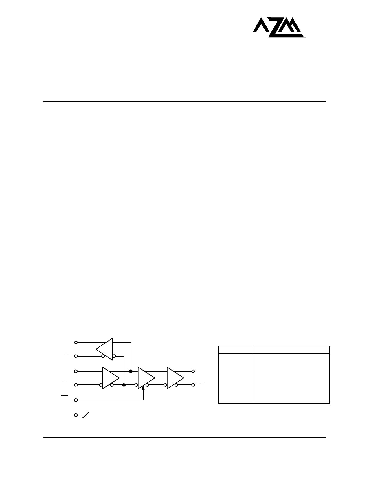
The AZ10/100EL16VO is a specialized oscillator gain stage with a high gain output buffer including an enable.
The QHG/Q¯ HG outputs have a voltage gain several times greater than the Q/Q¯ outputs.
The EL16VO provides an enable input (E¯N¯ ) that allows continuous oscillator operation. When E¯N¯ is LOW or
floating (NC), input data is passed to both sets of outputs. When E¯N¯ is HIGH, the QHG/Q¯ HG outputs will be forced
LOW/HIGH respectively, while input data will continue to be passed to the Q/Q¯ outputs. The E¯N¯ input can be
driven with an ECL/PECL signal or a full supply swing CMOS type logic signal.
The EL16VO also provides a VBB output for a crystal bias node. The VBB pin can support 1.5mA sink/source
current. When used, the VBB pin should be bypassed to ground via a 0.01µF capacitor.
Any used output must have an external pull down resistor. For 3.3V operation, a 180Ω resistor to VEE is
recommended if an AC coupled load is present. At 5.0V, a 330Ω resistor is recommended for the AC load case.
Alternately, a 50Ω load terminated to VCC – 2V may be driven directly. Unused outputs may be left floating (NC).
NOTE: Specifications in ECL/PECL tables are valid when thermal equilibrium is established.
1630 S. STAPLEY DR., SUITE 125 • MESA, ARIZONA 85204 • USA • (480) 962-5881 • FAX (480) 890-2541
www.azmicrotek.com
Share Link: 